

Overview
PhotoCAD stands as the advanced photonic IC layout design tool in today's market. Combining powerful script-driven capabilities with a user-friendly interface, it offers efficient management throughout the entire photonic chip design process. As photonic technology becomes increasingly complex, traditional design tools no longer meet the demands of modern designers. The emergence of PhotoCAD fills this gap, providing designers with a comprehensive, flexible, and efficient solution, radically transforming the landscape of photonic chip design.
Introduction
With the advent of early market-leading tools, code-driven layout methods have been widely adopted in photonic chip design. However, as the complexity of photonic chips continues to grow, designers urgently need more advanced code-driven solutions to address ongoing challenges.
Features
Compared to the current mainstream tools, PhotoCAD excels in several key areas, quickly establishing itself as the top choice for photonic chip layout design:
Unparalleled Flexibility: PhotoCAD offers enhanced customization capabilities, especially in the area of optical waveguide linkers, providing the necessary flexibility for complex designs.
Simple and Intuitive User Experience: All parameters in PhotoCAD are clearly displayed, eliminating the need for deep searches. This approach not only boosts efficiency but also reduces risks in the design process. Designers can work with more confidence, fully mastering the tools they use. For example, definitions related to the process and layers can be easily seen and customized in layers.py.
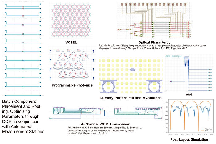
Cutting-edge Automatic Routing Technology: PhotoCAD's automatic routing technology is at the international forefront. The software features functions like Auto-transition, Auto-bend, Auto-expand, and Auto-taper. Moreover, it allows users to set pass-points for routing avoidance.Comprehensive PDK Integration: Although PhotoCAD is relatively new, it enables users to easily edit CSV files to import PDK process layers, allowing layout design based on foundry processes. This stands in stark contrast to most traditional tools that offer only a limited number of pre-built PDKs.
Advanced Simulation Capabilities: Powered by pSim, PhotoCAD provides powerful time-domain, frequency-domain, and eye diagram analysis simulations, surpassing the capabilities of other tools.
Integrated Toolchain: PhotoCAD provides a complete toolchain for users, from layout to schematic, and then to SDL-based script generation, on par with the three major EDA tools and even more comprehensive than PDA.
In summary, with its technological edge, PhotoCAD has emerged as a more advanced option for photonic chip design compared to traditional tools. It signifies the dawn of a new era in code-driven layout technology.