
Temperature Compensation Technology for CMOS-MEMS Monolithic Integrated Calorimetric Flow Sensing System
- Latitude Design Systems

- Mar 24
- 4 min read
Introduction
Flow sensing technology has wide applications in industrial monitoring, medical diagnostics, and other fields. With the increasing demand for precise flow measurement, especially in applications such as respiratory monitoring during health crises, high-precision flow sensors with temperature compensation functionality have become particularly important. This article references the latest research on the design and implementation of a CMOS-MEMS monolithic integrated calorimetric flow sensing system-on-chip (SoC) with built-in temperature compensation [1].

System Architecture and Basic Principles
The core innovation of this flow sensing system lies in the monolithic integration of MEMS sensors with CMOS circuits. The system is fabricated using P+ polysilicon layer technology and consists of a central heater and symmetrically distributed thermistors. This integration significantly improves the signal-to-noise ratio while optimizing chip area utilization and reducing overall development costs.

The sensing mechanism is achieved by strategically placing upstream and downstream thermistor pairs (Ru1, Ru2, Rd1, and Rd2) around the central heater (Rh). When gas flows through the sensor, a temperature difference is generated between the upstream and downstream thermistors. This temperature difference is converted into an electrical signal through a precision readout circuit. The system is fabricated using SMIC 0.18 μm 1P6M CMOS technology and integrates a variable temperature difference (VTD) control circuit along with a low-noise current feedback instrumentation amplifier (CFIA) readout circuit.
Temperature Compensation Strategy
Temperature drift is one of the main challenges faced by flow sensing systems, as it can affect measurement accuracy under varying operating conditions. The system employs an innovative VTD control circuit to address this issue. The VTD circuit operates in a negative feedback loop, where the resistance ratio R1/R2 and (Rr + Rc)/Rh in the Wheatstone bridge is configured as k = 5:1.

The operational amplifier (OPA) in the design achieves a high gain of 108.6 dB and a phase margin of 62.8°, ensuring stable and precise feedback. The VTD circuit can deliver a maximum power of 3.1 mW to the heater, which is significantly higher than the typical requirement of less than 1 mW for achieving a 50°C overheating condition. This power margin ensures stable operation across various flow rates and ambient temperatures.
Manufacturing Process and Implementation
The manufacturing process of this system precisely integrated CMOS technology with specialized MEMS process steps to realize a fully integrated sensing system. The fabrication process starts with standard CMOS technology, followed by dedicated post-CMOS steps to release the MEMS structures.

The manufacturing sequence includes several key steps, beginning with the preparation of the CMOS chip. Photolithography is then used to expose the top metal layer (M6) of the sensor's suspended region. This is followed by dry etching to remove the exposed top metal layer and reactive ion etching (RIE) to etch the silicon dioxide down to the silicon substrate. The process concludes with deep reactive ion etching (DRIE) to create vertical trenches and XeF2 plasma etching to suspend the sensor structure.
Experimental Setup and Verification
The experimental validation was conducted using a comprehensive test setup to evaluate the sensor’s performance under various operating conditions. The fabricated SoC was packaged inside a custom-designed 3D-printed flow channel measuring 65 mm × 12 mm × 2.5 mm (length × width × height) and embedded in a printed circuit board.

The test setup utilized nitrogen (N2) flow controlled by a pressure regulator and throttle valve. The entire setup was placed inside an environmental chamber (SH-222, ESPEC, Japan) to precisely control ambient conditions. Experimental results demonstrated significant improvements in temperature stability, with the compensation system reducing temperature drift from ±8.9% to ±1.6% within a flow velocity range of 0–10 m/s and an ambient temperature range of 0–50°C.
Performance Results and Analysis
The system’s performance was evaluated under various operating conditions, revealing complex behavior. In constant temperature difference (CTD) mode, the heater maintained a relatively stable overheating temperature of approximately 50°C. However, the system output exhibited noticeable variations with changes in ambient temperature, showing a ±7.9% deviation at 9 m/s relative to the output at 25°C.
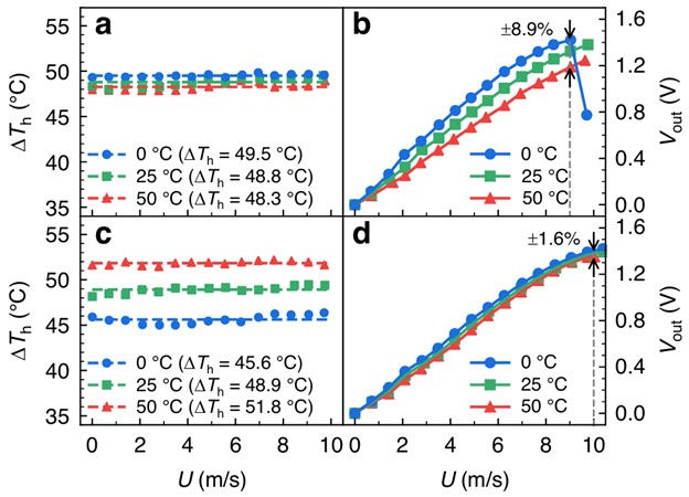
The implementation of the VTD mode led to significant improvements. The compensation strategy utilized a carefully selected compensation resistor Rc, which had a resistance value of 748.21 Ω at 25°C with a temperature coefficient of 3.037 × 10⁻³ °C⁻¹. This configuration was achieved by paralleling a PT100 resistor with a PT500 resistor, then connecting this set in series with another PT100 and PT500 resistor pair.
Conclusion
This integrated system exhibits significant advantages for medical applications, particularly in respiratory monitoring. The monolithic integration approach reduces system size and lowers costs. The system's performance characteristics include a wide operating range (0–10 m/s), low power consumption (<0.92 mW heating power; <4.96 mW system power), and a fast response time (87.5 ms). The successful implementation of on-chip temperature compensation eliminates the need for external calibration or compensation circuits, greatly simplifying system integration and enhancing reliability.
References
[1] L. Hong, K. Xiao, X. Song, L. Lin and W. Xu, "System-level modeling with temperature compensation for a CMOS-MEMS monolithic calorimetric flow sensing SoC," Microsystems & Nanoengineering, vol. 11, no. 13, pp. 1-11, Jan. 2025, doi: 10.1038/s41378-024-00853-8.


Comments