
Introduction
Single-Photon Avalanche Diodes (SPADs) have become essential photodetectors for applications such as time-of-flight measurement, facial recognition, and telemetry, thanks to their high sensitivity and speed in the near-infrared domain. One of the key figures of merit for SPAD devices is the Photon Detection Probability (PDP), which represents the SPAD's sensitivity and is defined as the probability of an absorbed incident photon generating an avalanche event.
In this article, we will explore an innovative approach to improve the PDP of SPADs integrated into Fully Depleted Silicon-On-Insulator (FD-SOI) CMOS technology. By nanostructuring the Shallow Trench Isolation (STI) layer above the photosensitive zone, we can generate constructive interferences and consequently increase the light sensitivity for frontside illumination.
SPAD FD-SOI Architecture and Constructive Interferences
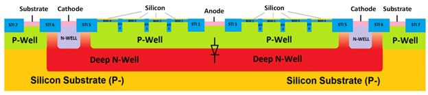
The SPAD FD-SOI is implemented below the buried oxide (BOX) layer, while the electronic logic circuits are inserted into the thin silicon layer on top of the BOX layer, providing an intrinsic 3D stack and a higher fill factor for backside illumination (BSI). However, for frontside illumination (FSI), the presence of Back-End-Of-Line (BEOL) layers can adversely affect light transmission.
To improve the PDP for FSI, we can exploit the STI trenches present in the SPAD cell due to the design rules of the technology. By optimizing the STI layer layout (size and period), we create a photonic crystal layer (diffraction grating) that generates constructive interference effects, locating the maximum interference in the Space Charge Region (SCR), where the avalanche triggering probability is highest.
Figure 1 illustrates the schematic cross-section of a SPAD FD-SOI and the concept of constructive interferences with STI patterning.
STI Nanostructuration Optimization
The optimization process involves two steps: finding the optimal fill factor (FF) of the STI pattern to maximize light transmission and extracting the optimal spatial period to achieve constructive interferences in the SCR.
In the first step, various FF values are simulated at specific wavelengths to determine the antireflection effect of the patterned STI compared to the reference structure. Figure 2 shows the profiles of the electric field magnitude and photogeneration rate, demonstrating the significant antireflection effect of the patterned STI.

The second step focuses on optimizing the pattern period to locate the maximum interferences in the SCR. Numerous simulations are performed, varying the pattern period for each FF value. Figure 2 illustrates the cartography of the photogeneration rate with a periodic pattern, clearly showing the diffracting effect of the pattern and the presence of a hotspot in the SCR.
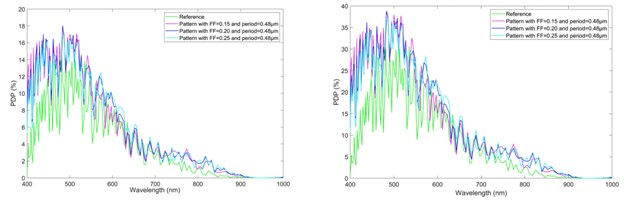
These simulations are then extended to a larger range of wavelengths (400-1000 nm) to investigate the improvement with visible to near-infrared light. Figure 3 presents the PDP profiles for different excess voltages, showing a clear relative improvement in the PDP for shorter and longer wavelengths, with the potential for a 700% relative gain at specific wavelengths and an average relative gain over 100% in the considered wavelength range.
Test Chip Presentation
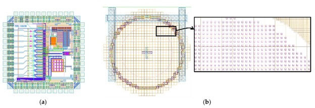
A test circuit was designed and fabricated in 28 nm CMOS FD-SOI technology, incorporating several variants of SPADs (reference, STI patterning with various FF, etc.) with associated electronics for active quenching and recharging. Figure 4 shows the layout view of the test chip and an example of a SPAD cell layout with inset zoom showing the STI patterning above the photosensitive area.
Experimental Results and Discussion
Dark Count Rate (DCR) Experimental Results:
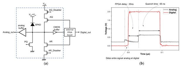
The DCR, which represents the noise level of the SPAD, was measured for the reference and patterned SPADs. Figure 6 shows the measured DCR as a function of excess voltage and temperature, revealing an increase in the DCR with excess voltage due to afterpulsing runaway for the patterned SPADs.
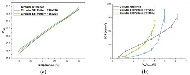
The Arrhenius plots in Figure 7 suggest that the noise mechanisms are a combination of thermal generation and band-to-band mechanisms associated with field-enhanced trap-assisted tunneling effects.

Photon Detection Efficiency (PDP) Experimental Results:
The experimental PDP was obtained using an integrating sphere setup, and the benefit of STI patterning compared to the reference SPAD is confirmed in Figures 8 and 9. Table 1 summarizes the PDP relative gains at peak sensitivity and the average PDP relative gains along the spectrum for different excess voltages and FF linked to the STI patterning.
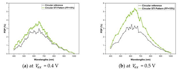
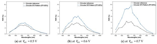
Table 1 summarizes experimental PDP relative gains for various excess voltages and fill factors.
Fill Factor | Relative Gain at Peak Sensitivity ( λ~645 nm) | Average Relative Gain in the Range [400-1000 nm] |
FF = 15% | 28% @ vex = 0.4 V 62% @ vex = 0.5 V | 33% @ vex = 0.4 V 55% @ vex = 0.5 V |
FF = 25% | 23% @ vex = 0.5 V 65% @ vex = 06 V 131% @ vex = 0.7 V | 12% @ vex = 0.5 V 53% @ vex = 0.6 V 116%@ Wx =o.7V |
Discussion
The experimental increase in the PDP for the patterned structure confirms the benefits of constructive interference achieved through STI nanostructuring. However, the measured improvement in the PDP is larger than the simulated values, which could be attributed to factors such as the consideration of normal incidence in simulations, the approximations made in quantifying photogenerated carriers outside the SCR, and the potential contribution of afterpulsing to the overestimation of the PDP gain.
Despite the significant improvement in the PDP, the absolute values remain lower than the state-of-the-art SPADs due to the use of a standard CMOS process without photonics-dedicated features like antireflective coatings or micro-lenses. Nevertheless, the STI nanostructuring approach would be even more effective if implemented in a process optimized for photonics applications.
Conclusion
In this article, we explored an innovative approach to improve the Photon Detection Probability (PDP) of Single-Photon Avalanche Diodes (SPADs) integrated into Fully Depleted Silicon-On-Insulator (FD-SOI) CMOS technology. By nanostructuring the Shallow Trench Isolation (STI) layer above the photosensitive zone, we generated constructive interferences, increasing the light sensitivity for frontside illumination while maintaining an equivalent Dark Count Rate (DCR).
Through simulations and experimental results, we demonstrated the potential of this approach to achieve significant relative gains in the PDP, particularly at shorter and longer wavelengths. While the absolute PDP values remain limited by the use of a standard CMOS process, the STI nanostructuring technique holds great promise for further performance improvements when combined with photonics-dedicated processes.
This study paves the way for the development of high-performance SPAD arrays with enhanced sensitivity for a wide range of applications, including time-of-flight measurement, facial recognition, telemetry, and scientific and medical imaging.
Reference
[1] S. Gao, D.-T. Vu, T. Cazimajou, P. Pittet, M. Le Berre, M. Dolatpoor Lakeh, F. Mandorlo, R. Orobtchouk, J.-B. Schell, J.-B. Kammerer, et al., "Shallow Trench Isolation Patterning to Improve Photon Detection Probability of Single-Photon Avalanche Diodes Integrated in FD-SOI CMOS Technology," Photonics, vol. 11, no. 526, Jun. 2024. [Online]. Available: https://doi.org/10.3390/photonics11060526.
Comments