
Introduction
The number of components integrated onto a single photonic integrated circuit (PIC) is rapidly increasing, mirroring the famous Moore's law trajectory observed in microelectronics. However, most of the very-large-scale integration (VLSI) PICs demonstrated so far consist primarily of passive components like waveguides and couplers, lacking the rich mix of active elements like lasers, modulators, and amplifiers. Emerging applications in communications, computing, and sensing will greatly benefit from high-density integration of both active and passive photonic components. Among various PIC platforms, indium phosphide (InP) offers the most comprehensive portfolio of active components alongside well-developed passive waveguiding capabilities. This tutorial explores the perspectives and technological advancements for scaling InP-based PICs toward large-scale integration (LSI) and VLSI.
PIC Scaling Trends
The evolution of component counts and die sizes of PICs reported over the past few decades is shown in Figures 1 and 2, respectively. Historically, InP has been the dominant platform, transitioning from small-scale integration to medium-scale integration in the early 2000s, driven by wavelength-division multiplexing (WDM) for optical communications. Recently, VLSI passive circuits with over 100,000 components have been demonstrated on the silicon photonics platform for applications like optical switches and optical phased arrays.
However, the packing density of active components like modulators and semiconductor optical amplifiers (SOAs) has not kept pace with passive elements (Fig. 3). This density gap between actives and passives is a critical bottleneck restricting further VLSI scaling and functional enhancement of PICs.


Component Miniaturization with InP Technology
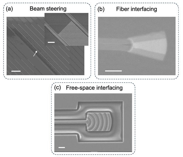
One key approach to scaling InP PICs is through component miniaturization, which can be achieved by substrate removal to create a high-confinement membrane waveguide structure, analogous to the silicon-on-insulator (SOI) platform. Figure 4(a) illustrates the waveguide cross-sections of conventional substrate-based InP and the membrane-based approach developed at TU Eindhoven. The membrane waveguide's cross-sectional area is only ~5% of traditional InP waveguides, enabling ultra-compact passive components like 1 μm radius bends, 4 μm polarization rotators, and 3 μm reflectors, as shown in Fig. 4(b).

Active component miniaturization is also facilitated by the membrane approach. Compact phase shifters with lengths down to 13 μm have been demonstrated (Fig. 5a) by placing the heating element in close proximity to the highly confined optical mode. Modulators based on carrier accumulation in a capacitor structure show promising miniaturization, with half-wave voltage-length products (VπL) down to 0.9 V.mm reported. Leveraging the enhanced optical confinement, ultralow threshold membrane lasers with footprints an order of magnitude smaller than conventional designs have been realized. Double-pass membrane SOAs exploiting mode-division multiplexing offer the potential for further size reduction while maintaining high optical gain.

Nanophotonic approaches like slot waveguides, plasmonics, and photonic crystals present additional opportunities for component miniaturization beyond the waveguide cross-section scaling. Figure 7 shows examples of slot waveguide and plasmonic modulators on the InP platform, with state-of-the-art VπL values down to 0.44 V.mm demonstrated. Photonic crystal membrane lasers and SOAs with slow-light enhanced gain have also been reported, albeit mostly with optical pumping so far.

Areal Optimization
In addition to minimizing individual component footprints, areal optimization through advanced integration schemes and circuit layouts is pivotal for achieving high packing densities of active and passive components on InP PICs.
Conventional butt-joint regrowth for active-passive integration is limited by the edge growth rate enhancement effect, which degrades material quality near interfaces and constrains the minimum spacing between adjacent regrown areas. An innovative "open-mask" regrowth technique developed at TU Eindhoven (Fig. 8a) circumvents this limitation by decoupling the functional area size from the masked area during epitaxy, enabling arbitrary spacing between active components as illustrated in Fig. 8c.

Efficient heat dissipation is crucial for densely integrated active components like lasers and SOAs. Figure 9 shows the simulated temperature profiles of a dense SOA array with and without thermal shunting to the silicon substrate. Direct bonding to high thermal conductivity substrates and incorporation of metal shunts can significantly improve heat extraction.

Electrical I/O density is another potential bottleneck for areal utilization in complex active-passive PICs. Multi-layer front-side and back-side electrical transmission lines enabled by the membrane structure (Fig. 10) can alleviate this issue by providing additional routing resources and separating bias delivery from signal delivery.

Wafer Size Scaling
Most commercial InP PICs are currently fabricated on 100 mm wafers, but emerging VLSI applications may drive the transition toward larger wafer sizes like 150 mm and 200 mm to leverage economics of scale and advanced process equipment from the silicon industry. Table I summarizes the state-of-the-art and challenges for various approaches to realize large-area InP membranes, including flip-chip bonding, die bonding, wafer bonding, SmartCut, micro-transfer printing, and heteroepitaxy.
Table I. Technologies for expanding InP PIC wafer sizes.
Technology | Readiness | Wafer size (mm) | Key current challenges |
Flip-chip | High | 300 | High topology, throughput, inter-die mechanical conflict |
Die-bonding | High | 200 | Inter-die mechanical conflict |
Wafer-bonding | Mid | 75 | Demonstration of 100 mm and beyond |
SmartCutTM | Mid | 200 | Demonstration of epitaxy after substrate transfer |
µTP | Mid | 200 | Mechanical alignment |
Heteroepitaxy | Low | 300 | Electrically pumping and coupling to membrane waveguides |
Conclusion
Indium phosphide presents a unique opportunity for scaling photonic integrated circuits toward large-scale and very-large-scale integration with a diverse set of active and passive components. Membrane-based InP platforms enable cross-sectional miniaturization of components down to the diffraction limit, while innovative integration schemes like open-mask regrowth, thermal shunting, and multi-layer electrical I/O facilitate areal optimization for high packing densities. Emerging applications in communications, computing, and sensing will greatly benefit from the functional scalability offered by these technological advancements in InP photonic integration.
Reference
[1] Y. Wang, Y. Jiao, and K. Williams, "Scaling photonic integrated circuits with InP technology: A perspective," APL Photonics, vol. 9, no. 050902, May 2024. [Online]. Available: https://doi.org/10.1063/5.0200861
Comentarios