
Introduction
Photonic integrated circuits (PICs) have gained significant traction across various applications, ranging from optical communications and quantum technologies to artificial intelligence. However, a critical requirement for the widespread adoption of PICs is the availability of highly efficient fiber-to-chip coupling interfaces. Grating couplers, which can diffract light out-of-plane and couple it to optical fibers, offer a promising solution for dense integration and wafer-scale prototyping. Nevertheless, on low-index photonic platforms, such as silicon nitride (SiN) or thin-film lithium niobate (TFLN), the limited scattering strength has hindered the achievement of coupling efficiencies comparable to those attainable in silicon photonics.
In this tutorial, we will explore a flexible strategy for realizing highly efficient grating couplers on low-index photonic platforms. By combining self-imaging gratings designed with a negative diffraction angle and a metal back-reflector patterned underneath the grating structure using cryogenic deep reactive ion etching (DRIE), we can overcome the limitations of reduced scattering strength and achieve coupling efficiencies approaching unity. This approach relies neither on an optimal material refractive index nor on engineered film thickness and etching depth, making it transferable to various low-index platforms [1].
Theory and Design
Coupling Efficiency Components: The coupling efficiency of a grating coupler can be modeled as the product of three contributions: the scattering efficiency (η1), the bidimensional overlap integral between the diffracted optical beam and the fundamental light mode supported by the optical fiber (η2), and the directionality of the diffraction process (η3).
CE = η1 × η2 × η3
Scattering Efficiency and Modal Overlap: Near-unity scattering efficiencies (η1) can be achieved by designing grating couplers with a sufficient number of grating teeth, as long as back-reflections in the input waveguide are negligible. To optimize the modal overlap (η2), two conditions must be met: (a) the diffracted beam must feature a Gaussian-like profile, and (b) the mode field diameters (MFDs) of the radiated beam and the fundamental fiber mode must be identical along both longitudinal and transverse directions.
Self-Imaging Grating Couplers: To simultaneously achieve high scattering efficiency and optimal modal overlap, self-imaging grating couplers designed with a negative diffraction angle are employed. This design approach allows for a focusing effect of the Gaussian-like diffracted beam at a distance of approximately 100-200 μm from the circuit plane, precisely matching the spatial mode supported by an optical fiber.
Grating Design and Simulations: The grating couplers are designed for operation in the telecom C-band with TE-polarized light. The grating period, filling factor, and number of grating teeth are optimized using 2D finite-domain time-difference (FDTD) simulations and analytical formulas for Gaussian beam propagation.
The grating teeth are shaped as concentric circular arcs to match the circular wavefront of the beam and achieve a focusing effect along the transverse direction. The taper features an opening angle and length designed to match the MFD of the diffracted beam to the fiber mode in the transverse direction at the focal point.

(a) It illustrates the grating coupler along its longitudinal direction, highlighting the grating period, Λ, and a linear apodization on the filling factor (FF=d/Λ). This design ensures that light traveling through the device is emitted upwards in a Gaussian-like shape and focused at a specific distance above the circuitry plane. The diagram also shows an optical fiber placed at the beam waist, with various components labeled in red, including the waveguide (WG), grating, and taper connecting these elements.
(b) A three-dimensional view of the coupler shows grating teeth as concentric circular arcs, designed to focus the diffracted beam not only longitudinally but also transversely, thanks to the negative diffraction angle. The taper, with a 70° opening angle and a length matching the distance from the first grating tooth to the beam waist's longitudinal position, aids in achieving the desired mode field diameter (MFD) at the beam's focus point transversely.
(c) 2D Finite-Difference Time-Domain (FDTD) simulations at a wavelength of 1550 nm demonstrate the coupler's outcoupling efficiency, showing a diffracted beam with a -12° angle and a focus approximately 175 µm above the circuit plane.
(d) Simulated mode field profiles at the beam waist are compared with a Gaussian function corresponding to the MFD of standard single-mode fibers (SMF-28) at 1550 nm, indicating close alignment.
(e) Poynting flux spectra within the 1500–1600 nm wavelength range illustrate the distribution of optical power for upward and downward-diffracted light, light transmitted at the grating's end, and back-reflected light, with values normalized to the input power at the grating.
Fabrication
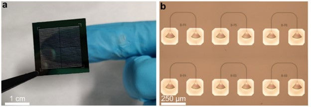
Starting Material and Preparation: The fabrication process starts with a 20 × 20 mm2 die consisting of a 330 nm thick SiN film deposited on a 3.33 μm thick SiO2 layer, thermally grown on a 525 μm thick Si handle. The die is annealed at 1100°C to reduce the absorption loss of the nitride film.
Cryogenic Deep Silicon Etching: A dense matrix of SiO2 membrane windows is patterned on the backside of the sample by photolithography and cryogenic DRIE of the silicon handle. Cryogenic DRIE enables the realization of membrane windows with nearly vertical sidewalls, a crucial requirement for accommodating grating couplers with a sizable number of grating teeth. This is a significant advantage over conventional wet etching methods, which produce angled sidewalls, limiting the maximum achievable size of the membrane.
Grating Coupler Patterning: The PICs, including the grating couplers, are fabricated on the SiN front side using electron-beam lithography with a negative resist, followed by reactive ion etching.
Metal Back-Reflector Deposition: Finally, an aluminum film is deposited on the backside of the sample by DC magnetron sputtering, serving as a metal back-reflector to enhance the directionality of the diffraction process.
Results and Discussion
Coupling Efficiency Measurements: The coupling efficiency of the fabricated grating couplers is measured using a V-groove fiber array equipped with SMF-28 fibers and featuring an 8° polishing angle. Continuous-wave laser light from a tunable laser source is coupled into the PIC via one of the grating couplers, and the transmitted light is recorded at the other coupler.
High Coupling Efficiency: With fully etched grating couplers fabricated on a 330 nm thick SiN film, a peak coupling efficiency of -0.55 dB (88% in a linear scale) is experimentally demonstrated in the telecom C-band.
Bandwidth and Reproducibility: While self-imaging grating couplers exhibit a narrower bandwidth compared to conventional designs, a high coupling efficiency can be recovered in the full telecom C-band by tuning the fiber position and optimizing the transmission with different alignment wavelengths.

Conclusion
In this tutorial, we have presented a flexible approach for realizing highly efficient grating couplers on low-index photonic platforms, such as SiN or TFLN. By combining self-imaging gratings designed with a negative diffraction angle and a metal back-reflector patterned using cryogenic DRIE, we have experimentally demonstrated a coupling efficiency of -0.55 dB in the telecom C-band. This strategy opens a practical path toward the realization of vertical couplers featuring coupling efficiencies approaching unity, a critical requirement for the implementation of scalable photonic technologies in various applications, including optical communications, quantum technologies, and artificial intelligence.
Reference
[2] Lomonte, E., Stappers, M., Krämer, L. et al. Scalable and efficient grating couplers on low-index photonic platforms enabled by cryogenic deep silicon etching. Sci Rep 14, 4256 (2024). https://doi.org/10.1038/s41598-024-53975-4
Comments