
Introduction
Visible-light photonic integrated circuits (PICs) hold immense potential for applications such as quantum information, biosensing, and scanning displays. However, extending the well-established silicon photonics platform to shorter wavelengths has been challenging due to the higher propagation losses encountered in the visible spectrum. Silicon nitride (SiN) has emerged as a leading material platform for visible integrated photonics owing to its wide transparency window, smooth etching, strong optical confinement, and foundry compatibility. Nevertheless, the propagation losses in SiN strongly depend on the film's deposition conditions and fabrication processes, making it difficult to identify the dominant source of loss and approach the platform's fundamental limits.
This tutorial article aims to provide a comprehensive understanding of the methods developed by Corato-Zanarella et al. to probe and minimize the propagation losses in SiN integrated photonics across the visible spectrum. We will delve into their innovative approach, leveraging ultra-high quality factor (Q) microresonators to discriminate and extract the absorption and surface scattering components of the loss. Additionally, we will explore their strategies for engineering the waveguide cross-section to approach the absorption-limited loss regime, ultimately achieving record-low propagation losses in high-confinement SiN platforms.
Loss Discrimination through Ultra-High Q Microresonators
Conventional loss measurement techniques, such as ellipsometry, cutback, outscattered light, and photothermal spectroscopy, cannot independently extract absorption and scattering losses or provide sufficient sensitivity for ultra-low loss thin films. Corato-Zanarella et al. overcame this limitation by employing ultra-high Q microring resonators fabricated with varying widths and radii, covering wavelengths from deep blue to near-infrared.
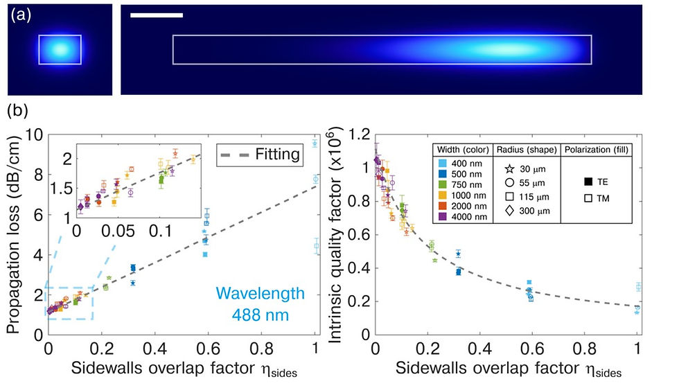
The key principle underlying their approach is that the modal overlap with the waveguide sidewalls decreases as the width and radius of the microresonator increase, thereby reducing the scattering loss and approaching the absorption limit. By measuring the Q factors of these resonators and fitting the propagation losses using a model that accounts for absorption, sidewall scattering, and top/bottom wall scattering, they could independently extract the absorption and scattering loss components with unprecedented sensitivity.
Figure 1(b) illustrates this concept, depicting the measured propagation losses and corresponding intrinsic quality factors as a function of the modal overlap with the sidewalls. The slope relates to the strength of surface scattering, while the intercept relates to material absorption, enabling the discrimination of these loss contributions.
Probing Loss Limits and Scaling Laws
Leveraging their microresonator-based characterization strategy, Corato-Zanarella et al. extracted the fundamental absorption and surface scattering loss limits of the SiN platform across the visible spectrum. They demonstrated that the material absorption follows a band-fluctuations model, as shown in Figure 2(a), and derived the optical bandgap (Eg = 4.63 eV) and Urbach slope (β = 5.07 eV^-1) of the SiN film.
The surface scattering loss, normalized by the modal overlap with the sidewalls, was found to follow a normalized version of the Payne-Lacey (NPL) model, which can also be well-fitted by a power law of the form λ^-2.3 (Figure 4(b)). From the NPL fitting, they extracted the root mean square (RMS) roughness (σ = 1.5 nm) and correlation length (Lc = 90 nm) of the waveguide sidewalls, consistent with direct measurements.
These scaling laws enable the determination of the necessary waveguide cross-section at a desired wavelength to achieve an absorption-dominated loss regime. Figure 2(c) illustrates how increasing the waveguide width reduces the surface scattering loss, ultimately approaching the fundamental absorption limit of the integrated platform.
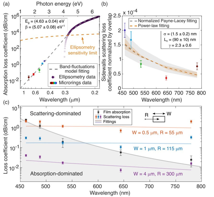
(a) The absorption loss coefficient is examined using ellipsometry, which shows accurate readings (opaque violet dots) down to its thin-film sensitivity limit (orange dashed line, k ≈ 0.002), below which film loss is underestimated (translucent violet dots). A band-fluctuations model fitting indicates an optical bandgap (Eg) of (4.63 ± 0.04) eV and an Urbach slope (β) of (5.07 ± 0.08) eV^−1.
(b) The sidewall scattering loss coefficient, normalized by modal overlap, is analyzed. Fitting with the NPL model estimates a root-mean-square (RMS) roughness (σ) of (1.5±0.2) nm and a correlation length (Lc) of (90±10) nm. A power-law fit (λ^−γ) determines γ = (2.3 ± 0.6), with shaded areas indicating fitting uncertainties.
Engineering Waveguide Cross-Section for Minimum Loss
By leveraging the derived loss scaling laws, Corato-Zanarella et al. engineered the waveguide cross-section to minimize propagation losses across the visible spectrum. They demonstrated record-low propagation losses for high-confinement SiN platforms, as shown in Figure 5(c), including 3.62 dB/m at near-infrared (780 nm), 6.0 dB/m at red (644 nm), 0.20 dB/cm at green (532 nm), 1.2 dB/cm at blue (488 nm), and 2.4 dB/cm at deep blue (461 nm).
These losses correspond to intrinsic quality factors as high as 2.07 × 10^7 (780 nm), 1.51 × 10^7 (644 nm), 5.7 × 10^6 (532 nm), 1.05 × 10^6 (488 nm), and 5.6 × 10^5 (461 nm). By employing a wide microring width of 4 μm, they minimized the surface scattering loss, allowing the propagation losses to approach the absorption limit of the SiN film (Figure 2(a)).
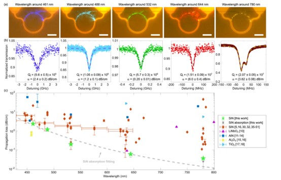
(a) Displays microresonators at resonance for wavelengths 461 nm, 488 nm, 532 nm, 644 nm, and 780 nm, with a 50 µm scale bar for reference.
(b) Reports the highest quality factors for fundamental TE modes in microresonators with a 4 µm width. The ring radius is 115 µm at 461 nm and 300 µm for other wavelengths, with error bars representing the mean ± standard deviation from tens of measurements for each resonance.
(c) Compares propagation losses with other state-of-the-art high-confinement platforms, highlighting that the studied SiN platforms exhibit the lowest losses to date, closely approaching the film's absorption limit as indicated by gray data points and dashed line from Figure 2(a).
Measurement Techniques for Visible Wavelengths
To accurately measure the ultra-narrow linewidths of the high-Q microresonators in the visible spectrum, Corato-Zanarella et al. developed a hybrid measurement technique combining microheater modulation and laser tuning, as illustrated in Figure 3. They modulated the microheater with a high-speed (10 kHz) and large-amplitude triangular voltage, while step-wise tuning the laser wavelength. This approach decoupled the resonance scanning speed from the wavelength tuning and measurement rates, enabling the extraction of ultra-narrow linewidths with high transmission sensitivity down to 2%.
The hybrid measurement technique overcame the constraints of typical sub-kHz laser modulation bandwidths and millisecond-long wavemeter exposure times, eliminating low-frequency noise that limits resonance visibility and extinction measurement sensitivity. Furthermore, their wavelength calibration method did not require knowledge of geometrical or material properties, making it applicable to any material platform and spectral range.
Conclusion
Corato-Zanarella et al.'s work represents a significant advancement in probing and minimizing propagation losses in integrated photonic platforms, particularly in the challenging visible spectrum. Their innovative approach, leveraging ultra-high Q microresonators, enabled the discrimination of absorption and surface scattering losses with unparalleled sensitivity. By deriving the scaling laws for these loss contributions and engineering the waveguide cross-section accordingly, they achieved record-low propagation losses in high-confinement SiN platforms across the visible spectrum.
The techniques developed in this work are crucial for the realization of large-scale, dense PICs and ultra-narrow-linewidth chip-scale lasers, paving the way for various applications in quantum information, biosensing, and scanning displays. Moreover, the measurement strategies and loss characterization methods are applicable to any material platform and spectral range, making them invaluable tools for pushing the boundaries of integrated photonics across the electromagnetic spectrum.
Reference
[2] Mateus Corato-Zanarella, Xingchen Ji, Aseema Mohanty, and Michal Lipson, "Absorption and scattering limits of silicon nitride integrated photonics in the visible spectrum," Opt. Express 32, 5718-5728 (2024)
Comments