
Introduction
Silicon photonics integrated circuits (PICs) have emerged as a promising technology for applications such as optical communication and sensing. One of the key passive components in silicon PICs is the waveguide crossing, which is necessary due to the single-layer nature of the silicon-on-insulator (SOI) platform. Various solutions have been proposed to achieve high-performance silicon waveguide crossings, including vertical coupling, multi-mode interference (MMI), beam synthesis, and particle swarm optimization (PSO).
While existing structures minimize the insertion loss (IL) per crossing, they are mostly designed for a narrow bandwidth. In this tutorial, we will explore a broadband silicon waveguide crossing enabled by curved subwavelength gratings (SWG) as lateral cladding, optimized through particle swarm optimization (PSO).
Design and Simulations
The waveguide crossing design is based on the 220 nm SOI platform with oxide top cladding. As shown in Fig. 1(a), the structure contains linear waveguide tapers from Wwg = 350 nm to W = 850 nm with a length of Lt = 4.81 μm, and curved SWG as lateral cladding.
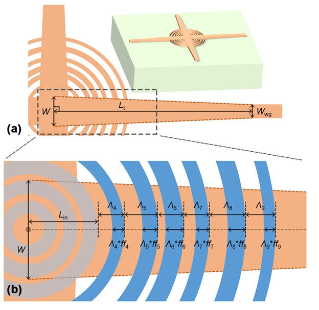
The original structure includes 9 SWG rings, and in this design, the periods and fill factors of the rings starting from the 4th one are separately adjusted through PSO. The first three rings remain the same as in the previous design, since they mostly overlap the waveguides.
The PSO algorithm is used to search for the sub-optimal combinations of periods {Λ4, Λ5, Λ6, Λ7, Λ8, Λ9} and fill factors {ff4, ff5, ff6, ff7, ff8, ff9}. The figure of merit (FOM) is defined as FOM = Tmin - CTmax - Rmax, where Tmin is the minimum transmission, CTmax is the maximum crosstalk, and Rmax is the maximum reflection of the device from 1260 nm to 1675 nm.
The impact of minimum feature size on the optimization process is also studied. Two PSO configurations are conducted: one with a minimum feature size of 60 nm and one with a minimum feature size of 45 nm. The best parameters found by PSO for each configuration are listed in Table I.
Table I: Best parameters found by PSO

The calculated results with the best parameters found by PSO are demonstrated in Fig. 2, along with the results of the benchmark design from the previous work. The PSO with a 60 nm minimum feature size achieves a maximum IL of 0.201 dB, a maximum crosstalk of -36.53 dB, and a maximum reflection of -21.03 dB over the 415 nm bandwidth.
![Calculated (a) IL, (b) crosstalk, (c) reflection spectra of the proposed waveguide crossing after PSO along with the benchmark design in [8], from 1260 nm to 1675 nm.](https://static.wixstatic.com/media/53b127_686ac90435464036aac9c9b27451d777~mv2.jpg/v1/fill/w_624,h_182,al_c,q_80,enc_auto/53b127_686ac90435464036aac9c9b27451d777~mv2.jpg)
The proposed method with a 60 nm minimum feature size reduces the maximum IL by 0.020 dB without affecting the crosstalk and the reflection compared to the benchmark. Furthermore, the maximum IL can be further reduced to 0.190 dB with a 45 nm minimum feature size, and the lowest IL reaches 0.080 dB. Although the maximum crosstalk with 45 nm features is higher than the benchmark, it is still below -30.84 dB, thus maintaining high performance. The 45 nm PSO also performs better in terms of reflection, with a maximum value of -26.15 dB, since the reduction of periods decreases the Bragg wavelength.
Conclusion
In this tutorial, we have explored a broadband silicon waveguide crossing based on particle swarm optimization of the subwavelength grating lateral cladding. By optimizing the geometry of each SWG ring separately through PSO, the design exhibits improved broadband performance compared to the benchmark, with IL < 0.190 dB, crosstalk < -30.84 dB, and reflection < -26.15 dB in simulations over a 415 nm bandwidth.
The proposed method demonstrates the potential of micro-engineering the SWG cladding index through PSO to further optimize the performance of silicon photonics components. This approach can be extended to other devices and applications, paving the way for more efficient and versatile silicon photonics integrated circuits.
Reference
[1] J. Zhang, W. Li, Z. Wei, and D. V. Plant, "Enhanced Broadband Silicon Waveguide Crossing Based on PSO-Processed SWG Cladding," Department of Electrical and Computer Engineering, McGill University, Montreal, Canada, 2024, pp. 1-6, doi: 979-8-3503-9404-7/24/$31.00 ©2024 IEEE.
Comments