
OFC2025|WDM Silicon Photonic Ternary Content Addressable Memory
- Latitude Design Systems
- 1 day ago
- 4 min read
Introduction
Content addressable memory (CAM) is becoming increasingly important for low-latency networking and computing operations, especially in applications requiring rapid network address lookups and similarity checks. While electronic CAM implementations struggle to exceed operation speeds of a few GHz, photonic implementations offer a promising alternative, enabling significantly faster search operations in the optical domain [1].

Overview of Photonic Ternary Content Addressable Memory Technology
Ternary content addressable memory (TCAM) enhances traditional binary CAM by allowing a third “don’t care” state (X) in addition to the conventional “0” and “1” states. This feature is particularly valuable in networking applications that require partial matches. Traditional electronic TCAM circuits face speed limitations and typically operate only at a few GHz, which has sparked interest in photonic alternatives.
The study presented in this paper demonstrates a silicon-integrated wavelength division multiplexing (WDM) TCAM cell capable of performing match-line operations at a record speed of 50 Gb/s, with energy efficiency as low as 38 fJ/bit. This performance is 2.5× higher than previous optical TCAM implementations operating at 20 GHz.
WDM TCAM Architecture and Operation Principle
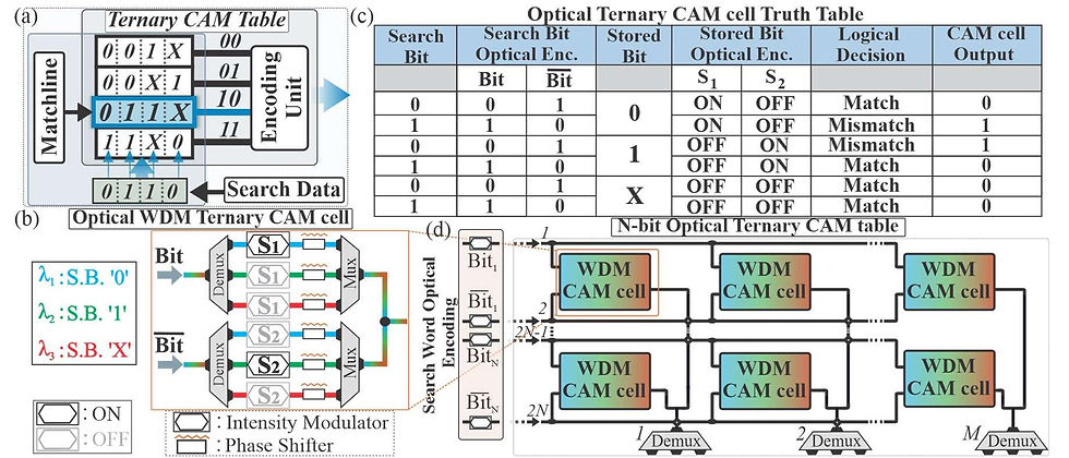
As shown in Fig.1(a), the TCAM table performs a multi-bit match-line (ML) comparison. In the illustrated example, a 4-bit search address ("0110") is broadcasted to every stored word in the TCAM table, with only entries containing the identical stored content generating a “match” signal.
The WDM TCAM cell configuration shown in Fig. 1(b) illustrates the circuit schematic for the three possible stored bit (S.B.) values: "0", "1", and ternary "X". The search bit and its complement bit̅ are encoded using NRZ format into a multi-wavelength optical beam injected into the TCAM cell. Each storage unit consists of two optical branches, incorporating demultiplexers that separate the wavelengths and forward the beams to their corresponding intensity modulators (IMs).
The S.B. value is encoded into the IM, with each value assigned a specific wavelength: λ1 for S.B. “0”, λ2 for S.B. “1”, and λ3 for S.B. “X”. The stored value is determined by the ON/OFF state of the IM. By properly adjusting the phase shifters, the resulting signals are multiplexed and recombined through coherent interference to compute the dot product between the stored vector and the search vector.
Experimental Implementation and Setup
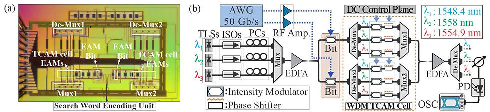
The photonic integrated circuit was fabricated using IMEC’s silicon photonics (SiPh) platform. It employed 56 GHz, 50 μm long SiGe electro-absorption modulators (EAMs) for both search and storage units, and thermo-optic phase shifters (TO PS) for coherent interference. The experimental setup in Fig. 2(b) uses three distinct laser sources emitting continuous wave beams at 1548.4, 1554.9, and 1558 nm.
The composite signals are injected into the TCAM via a TE grating coupler, then split using a 3-dB MMI coupler. An arbitrary waveform generator creates two complementary 50 Gb/s NRZ pseudo-random bit sequences, representing bit and bit̅. The modulated signals are demultiplexed, and each wavelength propagates through the respective EAM and PS modules to encode one of the three S.B. values.
Performance Results and Analysis

Fig.3(a) presents the synchronized time traces for the search input and TCAM outputs corresponding to the three S.B. values at 50 Gb/s. For S.B. “0” (when Bit=0 and Bit̅=1), the TCAM output drops to zero power, indicating a logical “match.” For S.B. “1,” a high-power level indicates a logical “mismatch.” The ternary “X” consistently yields a “match” regardless of the search input.
Fig. 3(b) shows the eye diagrams for all wavelengths validating each S.B. case, demonstrating clear eye openings for all search-storage configurations. Performance is evaluated using Q-factor measurements shown in Fig. 3(c), where the search bits exhibit Q-factors ranging from 5.8 to 7.62, highlighting the broadband capability of the EAM across a ~10 nm window. The storage cases for "0" and "1" exhibit Q-factors of 4.9 and 6.41, respectively.
Advantages and Future Impact
A key advantage of the proposed WDM-enhanced crossbar layout is its ability to encode all TCAM states using only one-third of the columns required in a conventional crossbar. Assuming a state-of-the-art insertion loss of 0.2 dB per Mux/Demux module, this architecture achieves over 60% reduction in insertion loss compared to traditional approaches.
Considering the CAM unit EAM responsivity of 0.8 A/W, input power of -4.5 dBm, and TO PS requiring 1.42 mW for π-phase shift, the WDM TCAM cell achieves an energy efficiency of 38 fJ/bit at 50 Gb/s.
This breakthrough demonstrates the potential of photonic TCAM to overcome the speed limitations of its electronic counterparts, offering a promising solution for high-speed networking and computing applications that demand low-latency search operations.
Reference
[1] T. Moschos, C. Pappas, S. Kovaios, I. Roumpos, A. Prapas, A. Tsakyridis, M. Moralis-Pegios, C. Vagionas, Y. London, T. Van Vaerenbergh, B. Tossoun, and N. Pleros, "A 50 Gb/s WDM Silicon Photonic Ternary Content Addressable Memory cell," in Optical Fiber Communication Conference (OFC), 2025, pp. Th1F.3.
Comments