Nature Communications Update | A New Chapter in Silicon Photonics: Research and Application of Heterogeneously Integrated Memresonators
- Latitude Design Systems
- Jan 30, 2024
- 4 min read
Abstract
In the emerging field of programmable photonics integrated circuits, there is a burgeoning interest due to their potential applications in deep neural networks, quantum computing, and field programmable gate arrays (FPGAs). However, these circuits face limitations due to the limited tuning speed and significant power consumption of current phase shifters. Addressing this challenge, the paper “Nature Communication” published in January in Nature Communications introduced the memresonator—a novel integration of a metal-oxide memristor with a microring resonator, serving as a non-volatile silicon photonic phase shifter. This device showcases impressive capabilities, including retention times up to 12 hours, switching voltages below 5 V, and enduring over 1000 switching cycles. Remarkably, the memresonator can be switched using voltage pulses as short as 300 ps, achieving a record-low switching energy of 0.15 pJ. Fabricated on a heterogeneous III–V-on-Si platform, these memresonators are capable of integrating a broad array of active and passive optoelectronic devices directly on-chip, thereby enabling in-memory photonic computing and significantly advancing the scalability of integrated photonic processors.
The increasing demand for high-performance computing systems capable of efficiently running artificial intelligence applications has escalated dramatically. This surge is primarily driven by the exponential growth in the usage of deep learning training programs, outpacing the rate of performance improvement predicted by Moore's law. Moreover, the real-time execution of learning algorithms on the massive volumes of data generated by interconnected smart devices within the Internet of Things (IoT) and edge computing scenarios necessitates advancements in hardware efficiency. Today's AI algorithms, utilized in applications such as autonomous vehicles and digital assistants, are predominantly implemented on neural networks inspired by the human brain's neuro-synaptic network, the epitome of energy-efficient computing. The commonly used hardware for these applications includes ASICs, GPUs, and FPGAs, with current electronic accelerators consuming about 0.5 pJ per multiply-accumulate operation, a fundamental neural network calculation.
Introduction
In the realm of modern computing, the quest for faster, more efficient memory solutions is relentless. The integration of photonic memory with computing architectures represents a paradigm shift, offering the promise of overcoming the limitations of traditional electronic memories. This tutorial article delves into a groundbreaking development in this field: a high-speed, energy-efficient non-volatile silicon photonic memory, leveraging the innovative concept of a heterogeneously integrated memresonator. This technology amalgamates the rapid, low-energy attributes of photonics with the non-volatility of resistive memory elements, setting a new benchmark for memory performance in computing systems. The significance of this advancement lies not only in its potential to enhance computational speeds and efficiency but also in its contribution to the evolution of computing architectures towards more sustainable and powerful systems.
Device Design and Fabrication
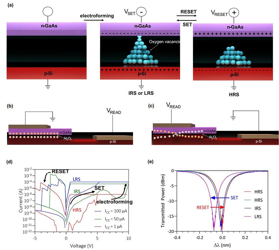
The memresonator device, a cornerstone of this innovative silicon photonic memory, exemplifies cutting-edge design and fabrication techniques in the integration of non-volatile memory with photonic structures. At its heart, the device employs a microring resonator coupled with a metal-oxide memristor, ingeniously integrated on a silicon substrate. This integration facilitates the modulation of light within the silicon photonics platform, harnessing the resistive switching properties of the memristor to achieve non-volatile memory functionality. The fabrication process meticulously combines silicon photonic fabrication norms with the deposition and patterning of memristive materials, ensuring seamless operational synergy between the optical and electronic components. This design not only underscores the feasibility of embedding memory directly within photonic circuits but also sets a precedent for the development of ultra-fast, energy-efficient computing systems.

Working Mechanism
The operational principle of the heterogeneously integrated memresonator is an elegant symphony of photonic and resistive switching technologies. At its core, the device utilizes a memristor whose resistance state is modulated by electrical signals. This change in resistance directly impacts the optical properties of an adjacent microring resonator, specifically its resonant wavelength, through the thermo-optic effect. When an electrical signal switches the memristor from a high to a low resistance state (or vice versa), it causes a corresponding shift in the microring's resonant frequency. This shift enables the encoding of data in the light passing through or coupled out of the resonator, thus achieving non-volatile memory functionality. This mechanism cleverly leverages the intrinsic properties of memristors and photonic structures to provide a memory solution that is not only fast and energy-efficient but also inherently compatible with silicon photonics platforms, heralding a new era of integrated photonic computing systems.

Applications and Future Directions
The advent of the memresonator heralds a transformative step forward for photonic computing, with applications that span across high-speed data processing, artificial intelligence, and neuromorphic computing. Its ability to provide fast, energy-efficient, and non-volatile memory is particularly well-suited for use in optical computing environments, where speed and efficiency are paramount. Looking ahead, the technology promises to open new avenues in the integration of photonic and electronic components, potentially leading to the development of fully optical processors and memory systems. Future research will likely focus on scaling these devices for larger memory arrays, improving the endurance and retention times further, and enhancing compatibility with existing silicon photonics platforms. This trajectory not only underscores the potential of memresonators in revolutionizing computing architectures but also points towards their role in enabling more sustainable, energy-efficient computing paradigms.
Conclusion
The development of the heterogeneously integrated memresonator represents a significant milestone in the evolution of photonic computing, merging the realms of non-volatile memory with high-speed, energy-efficient data processing capabilities. This technology not only demonstrates the potential for silicon photonic memories in future computing architectures but also sets the stage for further innovations in optical computing. As we continue to push the boundaries of what's possible within the computing landscape, the memresonator stands as a beacon of progress, heralding a new era of integrated, sustainable, and high-performance computing solutions.

Comentários