
IEDM2024|EDA Support for Scalable Disaggregated Systems
- Latitude Design Systems
- 2 hours ago
- 3 min read
Introduction
In the rapid evolution of semiconductor design, electronic design automation (EDA) plays a central role in enabling the development of modern scalable disaggregated systems. This paper explores the challenges, methodologies, and solutions in the context of 3DIC and system technology co-optimization (STCO) [1].

Evolution of EDA and System Architectures
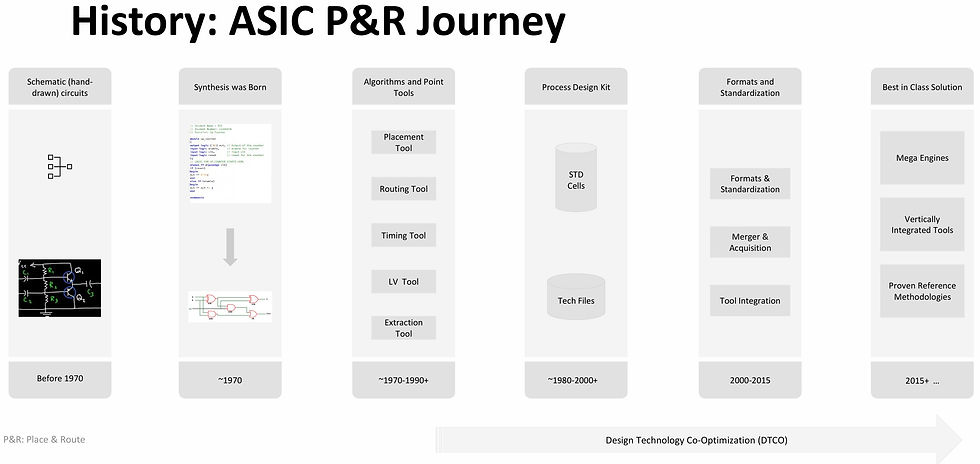
The semiconductor industry has progressed from traditional application-specific integrated circuit (ASIC) design methodologies to more complex disaggregated systems. As shown in figure 1, ASIC place and route (P&R) has evolved significantly from hand-drawn schematics before 1970 to modern design technology co-optimization (DTCO). This evolution demonstrates how EDA tools have adapted to increasingly complex design requirements.
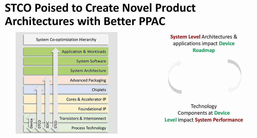
System architecture has evolved to accommodate new market demands and technological capabilities. Figure 2 illustrates the STCO hierarchy, showing the complex relationships among various system layers, from process technology to application workloads.
Disaggregated Architectures and Challenges
Disaggregated architecture represents a fundamental shift in system design. It is more than just a change in chip partitioning—it affects every discipline in silicon engineering. Key challenges include:
Main-band interconnect fabric architecture
Side-band fabric architecture (DFX, PM, Clock)
SoC topology and product configuration
Integration floor planning, power delivery, and thermal considerations
Test, verification, and manufacturing requirements

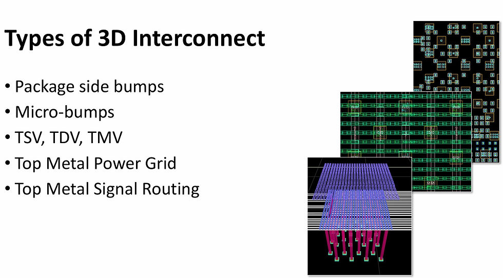
3D Interconnect Types and Implementation
Modern 3D systems employ various interconnect technologies:
Package-side bumps
Micro-bumps
Through-silicon vias (TSV), trough-dielectric vias, and through-mold vias (TMV)
Top metal power grid
Top metal signal routing
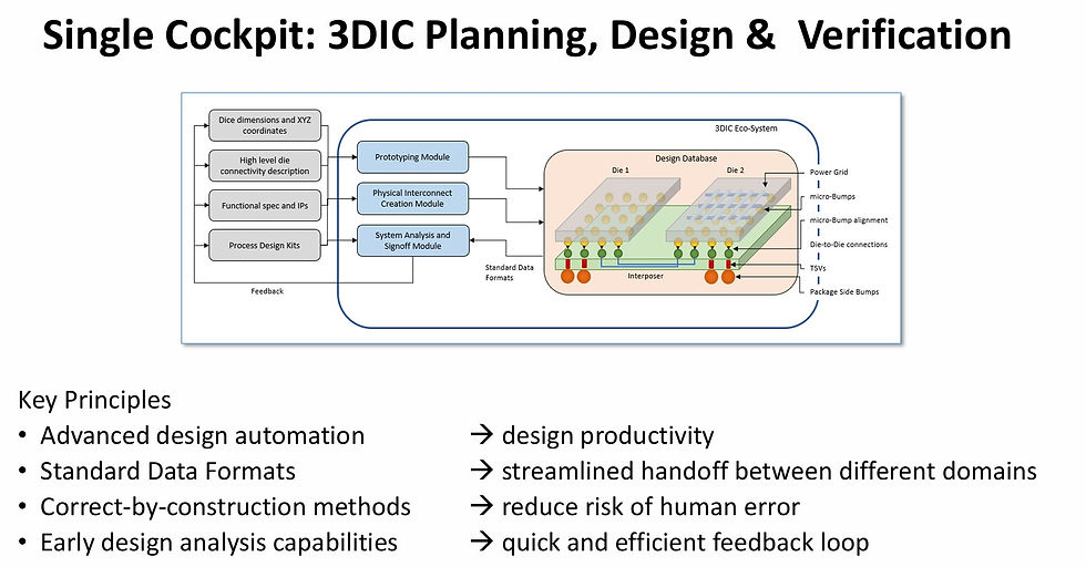
Optimization and Analysis Techniques
A systematic approach to 3D design optimization includes several key steps:
Early design space exploration
Initial bump placement
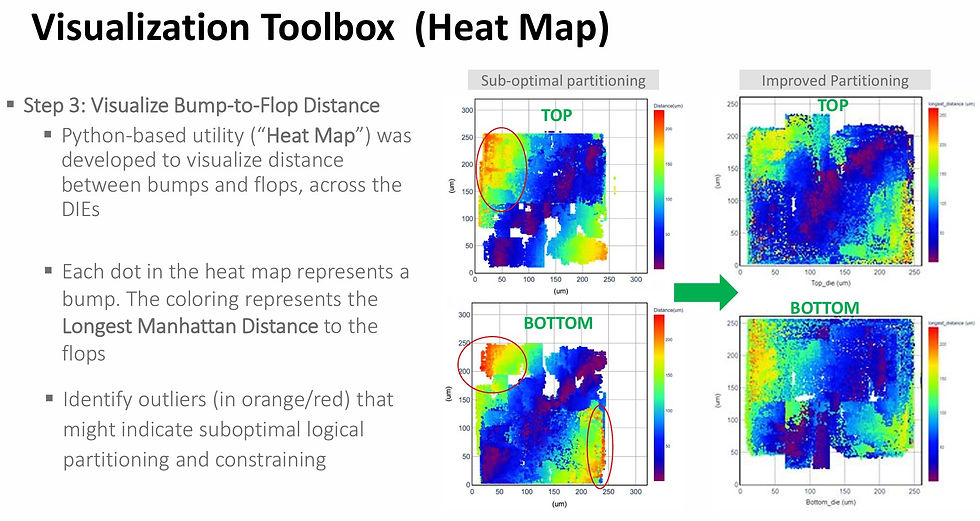
Bump-to-flip-flop distance analysis
Module alignment optimization
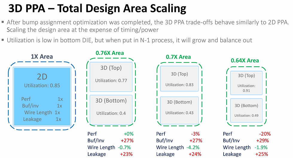
The optimization process includes careful consideration of metal layer scaling and area utilization. Figure 6 illustrates how different metal layer configurations impact performance and power metrics.
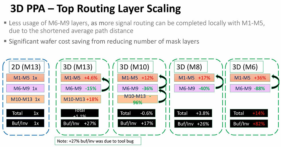
Performance, Power, and Area (PPA) Analysis
PPA analysis is critical to evaluating the effectiveness of 3D implementations. Key findings from the BZM test chip study include:
An average path delay reduction of 9% across over 100,000 register-to-register paths
Two fewer metal layers required on both top and bottom wafers
Significant improvement in area utilization and power efficiency
Future Directions and Challenges
The future of EDA for disaggregated systems focuses on several key areas:
Automated bump planning and optimization
Improved TSV placement and alignment
Enhanced top-metal routing for power and signal networks
Advanced signoff tools for early prototyping support
Integrated multi-physics analysis capabilities
As system complexity increases, the need for sophisticated automation and optimization techniques becomes even more critical. The focus remains on achieving peak performance in increasingly complex 3D integrated systems while managing power and area efficiency.
A comprehensive approach is required to integrate all aspects of design—from architectural planning to physical implementation—ensuring that the final design meets the stringent demands of modern applications while maintaining manufacturability and reliability.
Reference
[1] Evolution of ASIC design tools
Comments