Introduction
Heterogeneous integration is a key enabler for advancements in artificial intelligence (AI) and high-performance computing (HPC) hardware. This tutorial covers various aspects of heterogeneous integration technology, including die-to-die integration, substrate integration, co-packaged optics (CPO), and examples of state-of-the-art implementations.
Die-to-Die Integration Technology
Die-to-die integration is a crucial component of heterogeneous integration. The distance between electrical connections is minimized, or alternative routes like optical/wireless interconnects or CPO are utilized. SiPlus classifies die-to-die integration based on the elements involved: BEOL (Back-End-Of-Line), FEOL (Front-End-Of-Line), copper pillar, micro-bump, and TSV (Through-Silicon Via). This classification system is mapped to tradenames from different companies.


Several bonding approaches exist, such as face-to-face, face-to-back, and hybrid bonding. Hybrid bonding benefits technologies like High Bandwidth Memory (HBM).

Process for Heterogeneous Integration
The die-to-die integration process involves steps like RDL (Redistribution Layer) formation, wafer bumping, and assembly. The following illustrate various steps in this process flow.


Substrate Integration
Substrate integration is another critical aspect of heterogeneous integration. SiPlus proposes using a 2.XD structure to understand and classify different substrate integration approaches (Table 1).
Table 1. Conversion of Tradenames to 2.XD.
Company | Tradenames | 2.XD 2.XD-L: L means local | DF: Die First DM : Die Middle DL : Die Last |
tsmc | CoWoS-S | 2.5D | DM |
CoWOS-R | 2.2D | DM | |
CoWoS-L | 2.5D-L | DM | |
InFO-R | 2.2D | DF | |
InFO-L | 2.5D-L | DF | |
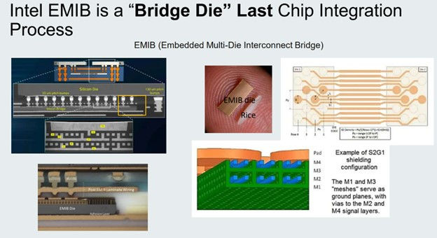
Intel | EMIB | 2.1D-L | DL |
IBM | DBHi | 2.1D-L | DL |
Samsung | I-CubeS | 2.5D | DL |
I-CubeE | 2.5D-L | DL | |
Siplus | eHDF | 2.0D | DL |
2.1D | 2.1D | DL | |
2.2D | 2.2D | DL | |
Integrated Bridge | 2.0-L | DL | |
Amkor | S-SWIFT | 2.2D | DM |
S-Connect | 2.5D-L | DL | |
SLIM | 2.0D-L | DL | |
ASE | eWLB | 2.2D | DM |
FOCOS | 2.2D | DM | |
SPIL | FO-EB | 2.5D-L | DL |
FO-MCM | 2.2D | DM | |
JCET | XDFOI 2.5D | 2.5D | DL |
XDFOI 2.1D | 2.0D | DL | |
Shinko | 2.1D type i-THOP | 2.1D | DL |
2.3D type i-THOP | 2.0D | DL | |
Unimicron | EIC | 2.4D | DL |
This classification system considers the integration of two components: dies (die-to-die integration) and substrates (substrate-to-substrate integration). The elements involved in substrate integration are BEOL/RDL, ABF/PP (Ajinomoto Build-up Film/Pre-Preg), TLV (Temporary Lattice Via), TSV, and solder.

SiPlus provides TSV-less integrated substrate solutions across the 2.XD spectrum, offering better electrical performance, cost-effectiveness, heat dissipation, and a lower carbon footprint compared to baseline approaches (Table 2).
Table 2. TXV-less 2.XD Integrated Substrate Solutions
2.0D S1 | 2.1D S2 | 2.2D S3 | 2.3D S4 (RDL+Coreless Substrate) | 2.5D S5 | |
Electrical Performance | Better than baseline(no solders, no TXVs) | better than base line | Slightly better than baseline | Slightly better than baseline | Baseline |
Cost | Better than baseline. (less direct and indirect materials and less assembly needed) | Comparable or better than base line | Comparable or better than baseline | Comparable or better than baseline | Baseline |
Heat dissipation | Better than baseline* (Thinnest in Z direction) | better than base line | Slightly better than baseline | Slightly better than baseline | Baseline |
Carbon Footprint | Best | Baseline |
Integrated Bridge Solution
SiPlus' Integrated Bridge Solution addresses the challenge of assembling multiple bridges for die-to-substrate interconnects. The bridges are lithographically defined and integrated, making it suitable for chiplet assembly requiring multiple fine-pitch bridges.

Large Substrates for AI
AI applications demand large substrate areas (e.g., 50x50mm, 100x100mm, 150x150mm, 200x200mm), fine RDL lines (10μm, 5μm, 2μm, 1μm, 0.5μm), excellent flatness, and reduced total thickness in the Z-direction for better electrical performance and heat transfer.
Copper Trace Formation
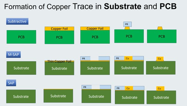
Subtractive, semi-additive (M-SAP), and full-additive processes are used for copper trace formation in substrates and PCBs. Improving copper trace quality involves addressing undercut, surface roughness, and dimension changes.

For fine lines, techniques like lift-off and CMP (Chemical Mechanical Planarization) processes are employed, enabling copper traces as fine as 1.7μm on double dielectric layers.


Dielectric materials with low dielectric constant, low dissipation factor, and low CTE (Coefficient of Thermal Expansion) are required for fine line formation.
Advantages of 2.0D Structure
The 2.0D structure, which combines thin-film RDL layers and ABF layers without solder in between, offers several advantages:
Uses less direct material (no TSVs, TLVs, or solder)
Fewer manufacturing processes (no TXV or soldering)
Reduced surface finishing layers
Better electrical and thermal performance
Die-last process benefits (higher yield, less testing)
Overall, a high-performance, low-cost, and low-carbon footprint solution
Substrate Flatness and Glass Core
Maintaining substrate flatness is crucial for fine-pitch requirements. SiPlus has demonstrated a 2.2D structure with a 60x60mm substrate, passing 1000X TCT reliability testing.

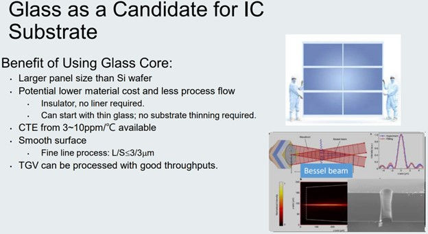
Glass cores offer advantages over organic cores, such as better dimensional stability, flatness, and potential for larger substrate sizes. Glass cores can enable higher TGV (Temporary Glass Via) density and reduced ABF layer requirements.


Co-Packaged Optics (CPO)
CPO technology is essential for high-performance data centers, enabling efficient data transmission and reducing energy consumption. Companies like TSMC, Intel, and Ayar Labs are developing CPO solutions.


Example: Apple M1 Ultra
The Apple M1 Ultra is an example of advanced heterogeneous integration, combining two M1 Max dies and 8 DRAM packages using TSMC's InFO-L (Integrated Fan-Out) technology. It features a silicon bridge (UltraFusion) connecting the two dies, fan-out RDL layers, embedded silicon capacitors, and a metal lid.

Possible Future HPC Structures
Future HPC structures may incorporate features like multiple HBM stacks, optical fiber interconnects, and embedded active networking chips.


Conclusions
Heterogeneous integration technology is crucial for AI and HPC hardware development. Key requirements include large substrate form factors with fine line capabilities, excellent flatness and warpage control, low dielectric constant and dissipation factor materials, and integration with CPO technology. The integrated substrate 2.XD family from SiPlus can meet these future AI substrate needs by reducing overall substrate height, providing good electrical and thermal performance, enabling large glass substrates with warpage control, and offering low-carbon footprint solutions. This is an exciting period for innovative structural, process, and material solutions in heterogeneous integration technology.
Reference
[1] D. C. Hu, "Review of Heterogeneous Integration Technology," presented at the 2024 International VLSI Symposium on Technology, Systems, and Applications (VLSI TSA), Apr. 22, 2024.

Comments