
Expanding the Capabilities of Integrated Photonics
- Latitude Design Systems
- Feb 13, 2024
- 8 min read
Abstract
Photonic integrated circuits (PICs) have primarily been developed for telecommunications, but emerging applications create opportunities in areas like spectroscopy, augmented reality, quantum technologies, and more. These applications operate across the ultraviolet, visible, and infrared wavelength ranges, necessitating new material platforms for low-loss waveguides. Techniques for on-chip light generation are also reviewed. Heterogeneous integration of III-V gain materials is positioned as the most viable approach to enable complex, single-chip photonic solutions with high yield and performance.
Introduction
For over 30 years, the development of photonic integrated circuits (PICs) has focused on meeting the needs of data and telecommunications. This has led to optimized solutions for wavelengths around 1310nm and 1550nm, where silica optical fibers have minimum loss. However, a range of emerging applications require operation at other wavelengths, expanding the necessary coverage of PICs from the ultraviolet (UV) to the infrared (IR) and visible spectrum between.
Applications like augmented/virtual reality (AR/VR), quantum computing, spectroscopy and biosensing, navigation systems, RF photonics, and optical atomic clocks have distinct requirements that drive the need for broadband PICs. Some key specifications are summarized in Table 1. For example, quantum technologies based on trapped ions/atoms or for manipulating entangled photon pairs operate at particular visible or near-infrared wavelengths dictated by the chosen ion/atom. Meeting the scaling demands of useful quantum computers greatly motivates increased photonic integration. Spectroscopic sensors need broadband tunable sources or frequency combs to identify target molecules via their optical resonances.
Advancing PICs to address these applications requires developing:
Passive waveguiding platforms across the spectrum from UV to IR
Methods for on-chip light generation across this wavelength range
Techniques to integrate active optoelectronic components like optical gain alongside these passive waveguides to create system-on-a-chip (SOC) photonic solutions
This paper reviews promising material systems for passive waveguides, approaches for spanning visible wavelengths through direct laser emission or frequency conversion, and methods to integrate III-V gain materials for complete photonic integration. Techniques assessed include hybrid assembly, photonic wire bonding, transfer printing, and heterogeneous integration. Among these, heterogeneous integration is argued to offer the best performance, reliability, and commercial viability for complex integrated photonic systems.
TABLE 1. Summary of some application drivers and specifications for some emerging market verticals [1]
Market | Application | Wavelength of operation | Key requirements | Driver |
AR/MR/VR | Displays | RGB (460–630 nm) | Very low on-chip loss/scattering, high-performance switching, high wall-plug efficiency | Integrated laser display engine for SWaP-C improvement |
AR/MR/VR | Sensing | 850–980 nm | Small size, high wall-plug efficiency, steering/reconfigurability of pattern | Pairing of photonic illuminators with CMOS camera for cost-efficient sensing |
Quantum computing | Trapped atoms/ions, generation of entangled photon pairs | ∼250 to ∼1700 nm depending on configuration | Generally, narrow to very narrow linewidth, low noise, high extinction ratio of on/off gating, very high signal to total spontaneous emission ratio, high quality filters, high density | SWaP-C improvement and enabling scaling of systems |
Quantum sensing | Magnetic field, electric field, temperature, gravity, force measurements, etc. | Various, often driven by atomic transitions | Narrow to very narrow linewidth, low noise, modulation for laser locking | SWaP-C and performance improvement compared to current systems |
Positioning, navigation, and timing (PNT) | Gyroscopes and optical clocks | Driven by atomic transitions, on-chip losses or fiber performance | Very narrow-linewidth (atomic, resonant), broadband (interferometric), very low on-chip propagation loss, very high level of polarization control, low coupling losses | SWaP-C and performance improvement compared to current systems |
Radio-frequency systems | Stable microwave oscillators, widely tunable microwave oscillators | N/A (output is RF), generally best performance where on-chip losses are lowest | Ultra-narrow linewidth (Hz-level of below), high-performance photodetectors (high-power, high-bandwidth), combs for downconversion | State-of-the-art phase noise performance, high-frequency performance, continuous tunability |
Spectroscopic sensors | Varies, depends on the specimen to be detected | Essentially all possible wavelengths, depending on application | Varies, but generally broadband operation is a requirement, comb-based sources are a plus (including dual-comb spectroscopy) | SWaP-C improvement compared to current systems |
Healthcare | Varies, depends on biomarker to be identified | Current systems utilize from ∼500 to 1700+ nm, broader operation beneficial | Varies, but generally broadband operation is a requirement | Continuous monitoring or home point of care, SWaP-C improvement |
Highly robust comm. systems | Very high temperature, uncooled communication systems (e.g., 125 °C) | ∼9xx nm wavelength range seems to be superior in terms of thermal performance | Very high temp lasing, medium to high bandwidths, WDM is a plus | Improved robustness communication systems for uncooled operation at extreme environments |
Passive Waveguide Platforms
The material platform selected for passive waveguiding plays a key role in achieving low optical propagation losses across the desired wavelength range. Figure 1 maps various material systems against target applications/wavelengths and the accessible optical bandgaps.
Silicon nitride (SiN) has emerged as the premier waveguiding material for many applications due to ultralow loss (<0.1 dB/m), broadband transparency spanning 400nm to >2μm wavelengths, and CMOS compatibility enabling leveraging of advanced silicon manufacturing ecosystems. Ultra-low loss silicon nitride waveguides (Figure 2) have enabled chip-scale III-V micro-lasers and frequency combs. Efficient operation for both χ(2) and χ(3) nonlinear processes has been demonstrated for frequency generation. The refractive index of SiN makes it less sensitive to fabrication variations. Exceptionally high uniformity and yield at 300mm wafer scale is now possible. With a simple deposition process using common silicon wafers, outstanding performance, and compatibility with electronics integration, silicon nitride arguably presents the most cost-effective solution for commercial widespread applications.


Tantalum pentoxide (Ta2O5) enjoys interest as an alternative waveguide material system primarily due to a lower thermo-optic coefficient compared to silicon nitride. This helps minimize thermo-refractive noise in integrated lasers. The high index contrast of Ta2O5 enables tight optical mode confinement for nonlinear optics in small physical device footprints. Efficient frequency comb generation has already been shown in Ta2O5 microresonators. Ultraviolet transparency theoretically down to 300nm makes Ta2O5 suitable for visible/UV applications. However, optical losses to date come nowhere close to record low-loss SiN waveguides. The low deposition temperature does help enable integration alongside other photonic components with a restricted thermal budget.
Lithium niobate (LiNbO3) possesses transparency from the visible to mid-infrared. With strong electro-optic, acousto-optic, nonlinear (χ(2), χ(3)), and photoelastic effects, LiNbO3 allows high-performance integrated optical modulators and efficient wavelength conversion. But issues around compatibility with standard microfabrication tools, cost of thin-film LiNbO3-on-insulator wafers, optical power handling concerns especially at shorter wavelengths, and temperature sensitivity persist. Nonetheless, the unique capabilities of LiNbO3 integrated photonics make it a good choice for specialized applications in classical and quantum photonics.
Other material platforms like aluminum nitride (AlN) or aluminum oxide (Al2O3) push further still into the ultraviolet spectrum below 300nm wavelengths. Ultimately, each material presents its own advantages and tradeoffs, so heterogeneous integration enables flexibly combining various passive waveguides with associated active optoelectronic components as needed.
On-Chip Light Generation
There are two ways:
Direct emission: This is the preferred way to make lasers at a particular wavelength, using materials such as GaN, GaAs, or InP. However, there is a gap in the green–yellow spectrum (535–630 nm) where direct emission cannot provide lasing. This is an area of active research to close the gap with LEDs or optically pumped sources.
Frequency conversion: This is another way to generate light in visible and NIR, using nonlinear processes such as frequency doubling, tripling, or optical-parametric oscillation. These methods require good phase matching and are sensitive to fabrication tolerances, which can limit the scalability and yield. This is the only way to access the green–yellow gap with PICs today.
Gain Integration Strategies
While passive waveguides and wavelength conversion offer important building blocks, active optoelectronic components like semiconductor optical amplifiers and lasers are essential for any complete photonic system-on-a-chip (SOC). Integrating these III-V devices alongside passive waveguides can be achieved through various techniques with different tradeoffs.
Hybrid integration leverages pick-and-place assembly to combine separately fabricated photonic dies at the packaging level. High performance is possible, but manually aligning each device prevents scaling to large volumes, limiting adoption for low-cost consumer applications. Reliability concerns also arise from integrating components with mismatched coefficients of thermal expansion.
Photonic wire bonding seeks to improve mode overlap between coupled components by using 3D nanoprinting to create optical bridges between diced chips assembled on a shared substrate. However, fabrication is challenging, especially for shorter visible wavelengths. The need for post-processing assembly also introduces scaling barriers to complex multi-die integration. There are currently no commercial electronic foundries pursuing this approach.
Transfer printing uses an elastomeric stamp and surface chemistry modifications to directly pick up and print thin film devices onto a common photonic substrate. But despite years of research, it has yet to transition beyond elementary demonstrations to complex integrated systems, especially those including optical gain or injection current. The reliance on thin film III-Vs also limits optical output power. As with nanowire bonding, transfer printing remains confined to academic circles without volume commercial adoption.
In contrast, heterogeneous integration has successfully transitioned multiple technological generations of InP lasers and amplifiers integrated on silicon photonic integrated circuits for telecommunications, first pioneered at UC Santa Barbara and now scaled to mass production at 300mm wafer fabs by Intel using a complementary metal-oxide-semiconductor (CMOS) foundry infrastructure. The approach bonds blanket III-V epitaxial layers onto completed passive waveguides before the III-V mesa devices and interconnects are defined lithographically (Figure 3).
This wafer-scale processing ensures precise alignment between coupled active and passive components. The III-V film thickness and epitaxial layer structure can be tailored to optimize performance based on the target wavelength and application. Bonded films exceeding 10μm enable high optical power output while maintaining compatibility with wafer-scale automated semiconductor tooling. Prescreening blank III-V donor wafers before die bonding improves yield by eliminating material defects. Wafer-level probe testing further ensures component performance uniformity across each batch.

These same CMOS-compatible heterogeneous integration techniques have now been extended to integrate high bandgap materials like GaAs and GaN light emitters on silicon nitride waveguides (Figure 4) to provide optical gain across visible and ultraviolet wavelengths. Meanwhile, the ecosystem of 300mm foundries capable of silicon nitride processing continues expanding thanks to widespread commercial adoption in applications like biosensing. The same economies of scale that drove down costs for silicon photonics are thus poised to accelerate heterogeneous integrated photonics in new markets.

Rather than transferring or bonding finished devices, heterogeneous integration forms optical gain components directly registered to the underlying passive waveguides on a wafer scale before the finished ICs are diced. This enables an unprecedented level of complexity in the photonic circuits produced. Even if some applications require specialized functionality not easily co-integrated with silicon nitride or silicon photonics, heterogeneous integration supports a mix-and-match Lego-like approach to fabricating sophisticated multichip photonic systems. The ability to combine various active III-V films and passive waveguides provides extensive flexibility while maintaining compatibility with standard lithographic processing.
The maturity and reliability of heterogeneous integration has been firmly established through years of technology development, intense qualification, and high-volume manufacturing for datacenter transceivers within Intel. There is substantial evidence it can deliver superior performance, yield, and scalability at lower costs compared to academic alternatives like transfer printing or photonic wire bonding. The industry-tested ecological supply chain for heterogeneously integrated photonics makes it the leading candidate to unlock the next wave of photonic integrated circuits serving new near-visible and infrared applications in augmented reality, quantum technology, optical atomic clocks, and biosensing.
Challenges and Roadmap for Visible Photonics
Despite tremendous excitement for augmented reality displays, quantum cryptography, integrated optical gyroscopes, and other applications across the ultraviolet, visible, and infrared spectral range, the commercial reality today is that outside of optical fiber telecommunications, most photonics markets remain small and fragmented. This poses difficulties in sustaining scalable manufacturing and foundry infrastructure. Identifying larger “killer application” vertical target segments would greatly motivate further research and development. Volume commercial success cases can validate technological approaches to inform future road mapping.
For example, AR/VR displays integrating PICs for RGB visible lasers or projectors could scale to millions of units for consumer adoption. Chip-scale lidar for autonomous vehicles likewise taps immense markets. Miniaturized quantum cryptography or random number generation products secure emerging blockchain infrastructure. Optical biosensors uniquely detect biomarkers linked to disease or environmental threats. Any of these includes multi-billion-unit opportunity to justify foundry investment in novel integrated photonic components and heterogeneous active-passive technologies.
Technologically, efforts continue towards advancing epitaxial growth techniques to completely close the green-yellow gap from ~550-590nm where direct III-V laser emission remains challenging. This promises electrically pumped lasers covering 370-1700+nm once fully realized. Lasers with enhanced temperature resilience also support uncooled photonic circuits in rugged environmental conditions.
Heterogeneous integration processes must expand beyond 850nm wavelength telecom lasers to absorb all relevant III-V materials such as GaAs, GaN, InP, and their alloys across the compound semiconductor family. This includes developing suitable etch chemistries, surface passivation treatments, and contact metallizations for high-bandgap heterostructures. Integrating dissimilar materials in an overlay requires managing thermal expansion mismatch. But the excellent reliability demonstrated for silicon photonics transceivers prove thermal budget compatible solutions exist.
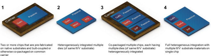
Future heterogeneous PICs may migrate towards co-packaged optical chiplets combining various functional wafer-scale integrated sub-systems as an intermediate step before advancing to full monolithic integration of multiple active materials on a common tri-layer passive waveguide substrate (Figure 5). Next-generation silicon photonic foundries promise this through silicon-based thin-film III-V epitaxy.
Conclusion
Silicon nitride passive waveguides offer broadband low-loss transmission spanning visible to infrared wavelengths, making this CMOS-compatible solution attractive for consumer augmented reality displays, biosensors, navigation gyroscopes, and quantum photonic technologies. Integrating incompatible materials like III-V compound semiconductors and lithium niobate via heterogeneous bonding techniques enables wafer-scale fabrication of finished photonic integrated circuits encompassing light generation, modulation, and detection. The reliability of this approach has been firmly demonstrated for silicon photonics transceivers. Extending heterogeneous integration up to visible wavelengths unlocks scalable integrated photonics for emerging applications and foundry-based manufacturing.
Reference
[1] Zhang, Chong, et al. "Integrated photonics beyond communications." Applied Physics Letters 123.23 (2023).
Comments