
Energy-Efficient Optical Transceiver Circuits Enabled by 3D Heterogeneous Integration
- Latitude Design Systems

- Aug 1, 2024
- 3 min read
Introduction
With the ever-increasing demand for high-speed data communication in modern computing systems, energy-efficient optical interconnects have become a crucial component. Heterogeneous integration strategies, such as high-density 3D bonding with a direct-bond interconnect (DBI) approach, offer significant improvements in optical transceiver density, optical modulation amplitude (OMA) sensitivity, and energy efficiency. This article presents a detailed overview of a 12nm optical transceiver that is co-designed with silicon photonic microdisk modulators/drop filters and 3D-integrated via DBI bonding.
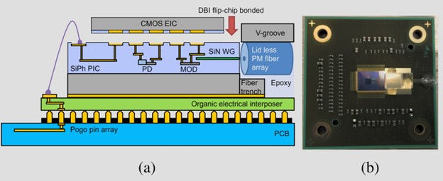
Introduction to 3D Heterogeneous Integration
The 3D heterogeneous integration of the optical transceiver involves the bonding of 12nm FinFET front-end circuits with silicon photonic microdisk modulators and drop filters. This integration approach, as shown in Fig. 1, enables the realization of a highly compact and energy-efficient optical transceiver module.
Optical Transmitter Architecture
The optical transmitter utilizes a low-power quarter-rate architecture, as illustrated in Fig. 2. This design approach relaxes the data path timing requirements and reduces the frequency of the clock distribution network, resulting in lower system and channel-level clocking power consumption.
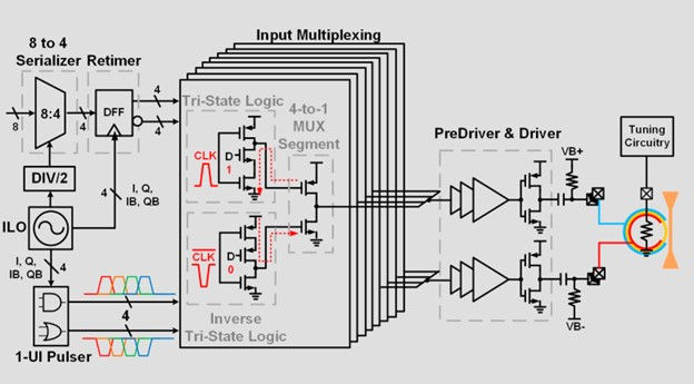
The transmitter serializes 8 parallel input bits through a combination of multiplexers and retiming circuits, culminating in a 4-to-1 serializer with 1-UI pulser circuitry and tri-state logic mux segments. The serialized data then passes through predriver buffers to the differential inverter-based output driver, which is AC-coupled to the microdisk modulator via an on-chip resistive bias-tee. This bias-tee allows for user-defined output common mode to reverse bias the modulator junction.
Experimental results demonstrate the transmitter's capability to achieve 12Gb/s and 18Gb/s PRBS-15 operation, as shown in Fig. 4(a) and Fig. 4(b), respectively. The transmitter consumes 157fJ/bit at 18Gbps with 1.2Vppd electrical modulation and a 7dB extinction ratio (ER).

Optical Receiver Architecture
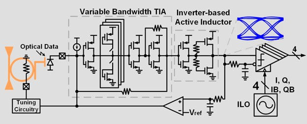
The optical receiver employs a variable-bandwidth transimpedance amplifier (TIA) for improved sensitivity, as depicted in Fig. 3. A programmable inverter-based active inductor at the TIA first-stage output enables bandwidth adjustment to compensate for chip fabrication/packaging variations' impact on input capacitance and feedback resistance.
A second active inductor at the input of the quarter-rate samplers further broadens the bandwidth at the sampling node. This dual active inductor design ensures broad bandwidth under a TIA front-end with a large feedback resistor, thus achieving high transimpedance, low input-referred noise, and proper bandwidth simultaneously without excessive power consumption overhead.
Additionally, an individual injection-locked oscillator (ILO) is included in each receiver channel to provide jitter-filtered 4-phase quarter-rate sampling clocks. An operational transconductance amplifier (OTA)-based offset calibration loop cancels the common mode offset of the TIA induced by the input photocurrent.
Experimental Results
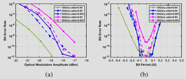
The optical receiver demonstrates impressive performance, achieving an OMA sensitivity of -18.8dBm at 18Gb/s, measured with optical PRBS-7 and 0.8A/W photodetector responsivity, as shown in Fig. 5(a). The receiver also exhibits a timing margin of 5.4% UI at 18Gb/s, as illustrated in Fig. 5(b). Furthermore, it is capable of operating at 25Gb/s with an OMA sensitivity of -17.0dBm.
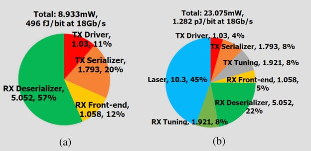
The receiver consumes 339fJ/bit at 18Gb/s, contributing to an overall energy efficiency of 496fJ/b from the transceiver circuitry alone. When including the source laser and microdisk tuning power, with an assumption of 30% wall-plug efficiency, the total transceiver power consumption is estimated at 1.282pJ/b, as shown in Fig. 6.
Conclusion
The co-design of 12nm FinFET front-end circuits with silicon photonic microdisk modulators and drop filters, integrated via the DBI 3D bonding approach, has enabled the realization of an energy-efficient optical transceiver. Leveraging low-parasitic 3D integration and low-power circuit design, this transceiver achieves an impressive 7dB extinction ratio and -17.0dBm OMA sensitivity at 18Gb/s, with sub-500fJ/bit energy efficiency. These advancements in optical transceiver technology pave the way for meeting the ever-increasing data communication demands of future high-performance computing systems.
Reference
[1] P.-H. Chang, P. Yan, A. Samanta, M. Fu, Y. Zhang, M. B. On, A. Kumar, H. Kang, I.-M. Yi, D. Annabattuni, D. Scott, R. Patti, Y.-H. Fan, Y. Zhu, S. J. Ben Yoo, and S. Palermo, "Energy-Efficient Optical Transceiver Circuits Enabled by 3D Heterogeneous Integration," presented at Texas A&M University and University of California, Davis, 2024.


Comments