
Introduction
Silicon photonic integrated circuits (Si PICs) have gained significant attention due to their potential for high-performance and cost-effective solutions. However, reducing the overall costs associated with the production and testing of these devices remains a crucial challenge. One approach to address this issue is by performing wafer-level testing until the final stages of the fabrication process [1]. This tutorial article introduces a coupling structure proposed by Eissa et al. [1] that combines both grating couplers (GCs) and spot-size converters (SSCs), enabling characterization of Si PICs through wafer-level and chip-level testing.
The Proposed Coupling Structure
The coupling structure presented in this work aims to reduce testing costs by utilizing wafer-level testing to estimate the characteristics of final chip-level devices. The structure consists of SSCs connected back-to-back and GCs, as shown in the inset of Fig. 1(a).
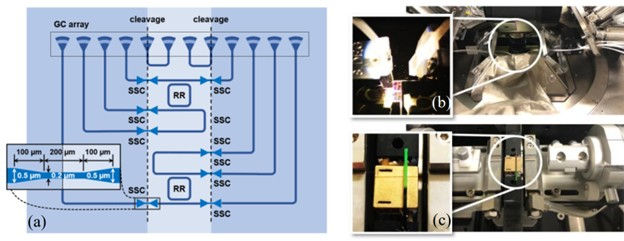
During in-situ fabrication or screening tests, the GCs connected to the PICs are used for wafer-level measurement. Once the packaging stage is reached after cleavage, edge coupling to fibers is carried out using the SSCs. By completing screening tests through wafer-level testing, only known-good-dies can be packaged, potentially eliminating some tests at the packaging level.

Proof-of-Concept Demonstration
To validate the proposed concept, ring-resonator (RR) devices were tested to evaluate the accuracy of the testing process. The setup included a 1×12 array of focusing GCs aligned with a fiber array of an automated wafer-level probing system, enabling in-process measurements via surface coupling. The GC corrugations had a period of 0.76 μm and a duty cycle of 50%. The GC array was connected to a 6×2 array of SSCs for chip-level measurements via edge-coupling by facet cleavage. The SSCs were introduced by tapering single-mode SOI waveguides from 0.5 μm to 0.2 μm over a taper length of 100 μm. The entire structure was fabricated on an SOI wafer with a top-silicon thickness of 220 nm using electron-beam lithography with a single-etching step of 190 nm depth.
Results
Figure 3 presents the wavelength spectra of the through and drop ports of the RR devices, obtained through surface-coupling via a wafer prober and edge-coupling via lensed fibers.
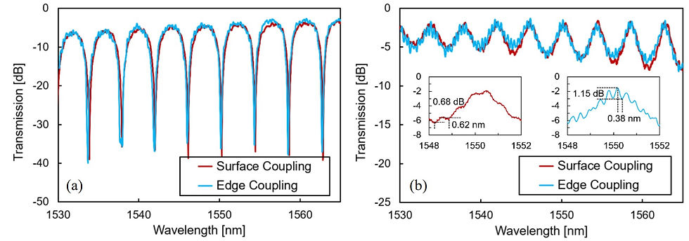
For surface-coupling measurements, a tunable laser diode was used to scan wavelengths while monitoring the received power. In the case of edge-coupling measurements, wide-band amplified spontaneous emission (ASE) light was injected, and the transmitted light was measured using an optical spectrum analyzer (OSA). The stage temperature was strictly maintained at 25°C, and coupling losses of reference waveguides were extracted and subtracted from the measurement spectra for normalization purposes (with 0.02 nm resolution).
The results demonstrated good agreement between wafer-level and chip-level measurements, although spectral ripples were observed due to minor reflections from GCs and cleaved facets, respectively. The minor free spectral ranges (FSRs) in Fig. 3(b) insets correspond to Fabry-Perot cavities formed by reflections between both input and output GCs and SSCs. The extracted ripple amplitudes correspond to effective reflectivities of 8% and 14% for surface and edge coupling, respectively. These ripples are expected to be minimized by using GCs with low backscattering and cleaved facets with anti-reflection (AR) coatings.
Conclusion
The proposed coupling structure combines GCs and SSCs, enabling the characterization of final chip-level Si PICs through wafer-level testing. The good agreement between wafer-level and chip-level testing results of RRs confirms that wafer-level testing can estimate chip-level device characteristics. This approach has the potential to reduce testing costs by utilizing wafer-level testing to screen and select
References
[1] M. Eissa et al., "Coupling structure for enabling both wafer- and chip-level characterization of silicon photonic integrated circuits," in IEEE Photonics Conference (IPC), 2024.
Comments