
Introduction
The semiconductor industry is undergoing a transformative shift towards an open chiplet ecosystem, where chiplets from different manufacturers can be seamlessly integrated into a single package. This transition promises unprecedented flexibility, scalability, and heterogeneous integration capabilities. However, realizing this vision is no small feat, as it requires overcoming a multitude of technical and business challenges. In this comprehensive guide, we'll explore the intricate process of co-optimizing the design and assembly of chiplet-based systems, shedding light on the key considerations and methodologies that pave the way for a successful chiplet revolution.
The Complexities of Chiplet Integration
At the heart of the chiplet ecosystem lies the need to align the diverse performance demands of end systems with the assembly and packaging capabilities of integrated device manufacturers (IDMs), foundries, and outsourced semiconductor assembly and test (OSAT) companies. This alignment is crucial to achieving acceptable yields and ensuring reliable operation under real-world workloads.
One of the primary challenges in chiplet integration is managing the thermal, mechanical, and electrical co-dependencies that arise when combining heterogeneous components. These interactions can lead to warpage, reduced yield, and reliability issues, necessitating meticulous design and assembly processes.
Additionally, the industry must navigate the legal and business complexities associated with packaging devices from multiple manufacturers within a single system. As Gabriela Pereira, a technology and market analyst at Yole Intelligence, notes, "The industry has understood that high-end advanced packaging technologies are needed to connect chiplets — but that's much more complex than it seems."
Tighter Collaboration and Customization
To unlock the full potential of the chiplet ecosystem, a paradigm shift in collaboration and customization is required. Traditionally, system design focused solely on meeting system requirements. However, in the chiplet era, design teams must consider a myriad of additional factors, such as signal integrity between dies, reliability, thermals, and more.
As Itai Leshniak, director of AI systems solutions at Applied Materials, explains, "Previously, when we designed a system, we only had to be worried about the system requirements. Once we start segregating into dies and reassembling them, we have to start looking at other things. We have to worry about putting them together while considering signal integrity between dies, reliability, thermals, etc."
This increased complexity necessitates tighter collaboration between foundries, IDMs, OSATs, and PCB manufacturers. Each chiplet-based system will require a customized assembly process, leading to a substantial growth in the number of assembly processes employed by OSATs. As one OSAT noted, among their ~5,000 customers, there are already ~1,000 different assembly processes.
The Role of Materials and Assembly Processes
Materials play a pivotal role in enabling new packaging technologies and enabling the integration of chiplets. As Tanja Braun, deputy group manager at the Fraunhofer Institute for Reliability and Microintegration IZM, states, "As you move into more advanced packaging, the process is getting much more complex because you are putting more things together. In the end, it's a combination of equipment, materials, and process development."
Three key thermal parameters must be considered when selecting materials for chiplet assembly: coefficients of thermal expansion (CTE), glass transition temperature (Tg), and thermal conductivity. These factors influence how a material behaves during manufacturing and packaging processes, as well as how it performs in the field.
Rama Puligadda, CTO at Brewer Science, highlights the challenges associated with material selection: "We have to ensure that the temperatures used for bonding materials don't exceed the thermal limitations of any of the chips that are being integrated into the package. Additionally, there may be some subsequent processes like redistribution layer (RDL) formation or molding. Our materials have to survive those processes."
Uniform heating during the reflow process is crucial to achieving optimal results and avoiding cracking. As Dick Otte, CEO of Promex Industries, emphasizes, "When you're taking it through a 250 degrees centigrade temperature change, then you need to heat up slowly so that the top doesn't get hot before the bottom does."
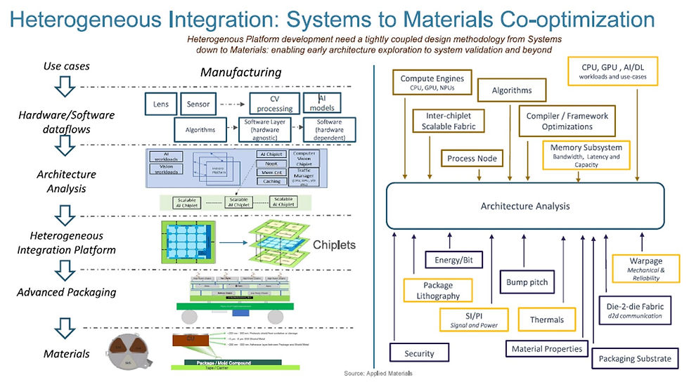
Leveraging Multi-Physics Modeling for Co-Optimization
To streamline the co-optimization process and reduce the need for empirical iterations, engineers are increasingly turning to multi-physics modeling. This approach enables a comprehensive understanding of the impact of material properties on the assembly process, power/thermals, and mechanical vibrations.
High-performance computing (HPC) chiplet products can consume up to ~1,000 watts at peak performance, underscoring the importance of thoroughly understanding power and thermal interactions. Marc Swinnen, director of product marketing at Ansys, explains their approach: "We work jointly with customers to develop a simulation flow that actually achieves what is needed now."
The simulation flow encompasses various aspects, including assembly stresses, mechanical vibrations, acoustics, and thermal analysis. "In the end, you're going to have to do physics simulation," Swinnen states. "We're trying to make it accessible to people in many different forms. But the bedrock of our tool offerings is that we have the meshing simulation and analysis."
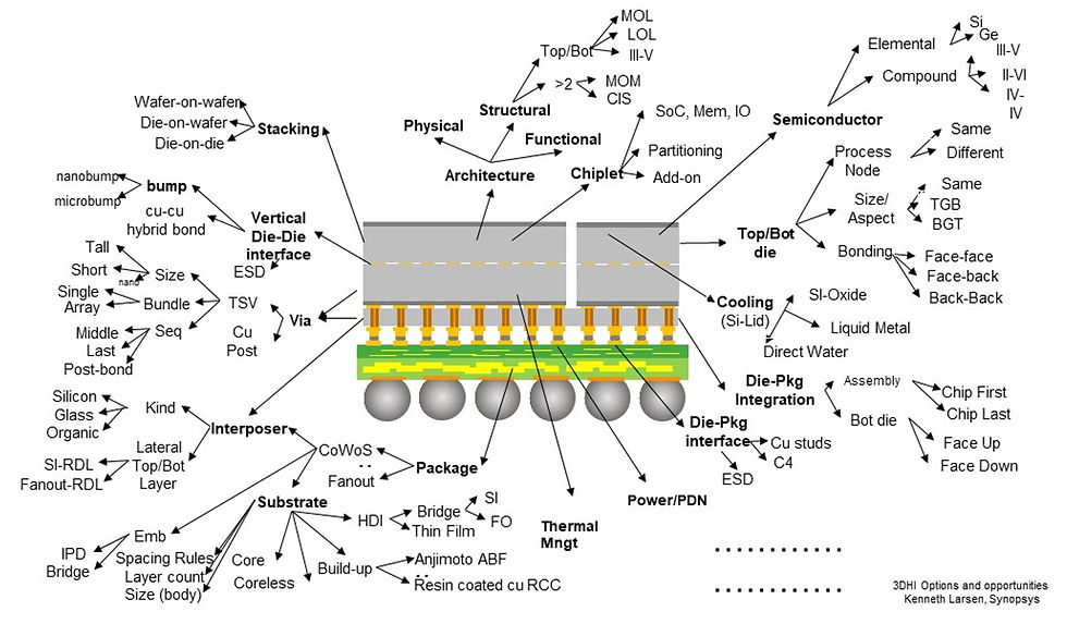
Evolving Assembly Design Kits (ADKs)
To navigate the complexity of chiplet-based designs, the industry is turning to assembly design kits (ADKs), which are akin to the process design kits (PDKs) used in conventional semiconductor design. ADKs capture design rules in an electronic format that can be imported into electronic design automation (EDA) tools, enabling seamless integration with design workflows.
However, the development of ADKs is still in its infancy, and their derivation and contents are currently in flux. Partnerships between EDA tool vendors, OSATs, and semiconductor device providers are essential for driving ADK standardization and maturation.
As Kenneth Larsen, director of 3D-IC product management at Synopsys' EDA Group, notes, "On the OSAT side, and maybe this is because it's so custom, design rules seem like a data sheet. Then you build and optimize the products over time or in collaboration with the OSAT. It's not an electronic exchange. In the IC world, this would be totally unheard of."
The current focus is on co-optimizing the system design with the chiplet assembly process, leading to an assembly process development flow (see Figure 3). This flow considers the need for customization of an assembly process and creates the necessary design rules for package designers.
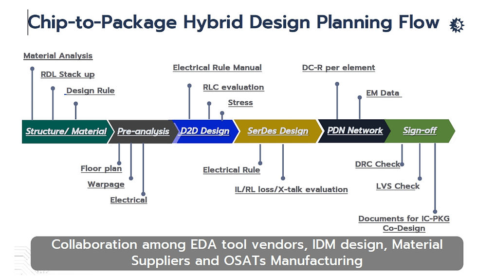
As Lihong Cao, senior director at ASE Group, explains, "First, you need to define your structure using chiplets. Are you using substrate RDL, 2.5D RDL, or a bridge? After that, you need to consider your structure's materials. What kind of material do you choose to fulfill your electrical performance and the mechanical stress requirements? After that, you do pre-analysis to ensure all the structures and materials you use are workable in terms of electrical, warpage, and mechanical stress."

Conclusion: Enabling the Open Chiplet Ecosystem
The transition to an open chiplet ecosystem is a monumental undertaking that requires close collaboration across the entire semiconductor supply chain. As Lihong Cao aptly states, "An integrated design and manufacturing ecosystem is important. It is very critical to have collaboration among IDM, vendors, materials suppliers. Everyone needs to work together to really enable integration for real applications."
By co-optimizing system architecture, materials, processes, and integration capabilities, the industry can pave the way for a future where chiplets from diverse sources can be seamlessly integrated, unlocking unprecedented innovation and performance gains. While challenges remain, the concerted efforts of industry stakeholders and the adoption of methodologies like multi-physics modeling and ADKs will be instrumental in realizing the full potential of the open chiplet ecosystem.
Reference
[2] Meixner, "What Works Best For Chiplets," April 18th, 2024. Online. Available: https://semiengineering.com/what-works-best-for-chiplets/
留言