
Double-Row CFET: An Innovative Architecture for Advanced Process Nodes
- Latitude Design Systems
- Mar 31
- 3 min read
Introduction
As semiconductor technology continues to evolve, size reduction and efficiency improvement remain primary objectives. This paper explores the double-row complementary field-effect transistor (Double-Row CFET) architecture in detail, outlining this semiconductor innovation and its advantages in performance, power consumption, and area optimization [1].

Evolution of Semiconductor Technology
Semiconductor technology has evolved from FinFET to nanosheet structures and has now entered the CFET era. This progression represents significant breakthroughs in semiconductor manufacturing processes.

This technological evolution is not only reflected in horizontal device scaling but also introduces vertical integration concepts, marking a fundamental transformation in transistor design and manufacturing technology.
CFET Architecture and Connection Schemes
The CFET architecture offers various innovative solutions for power and signal connections, forming the technological foundation for double-row CFET design.
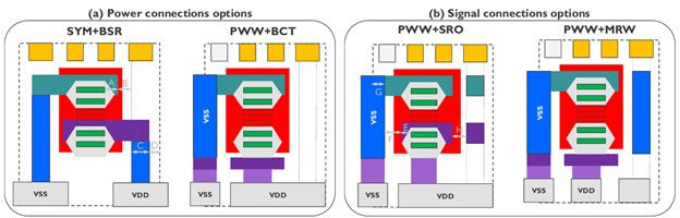
Among these, the PWW+MRW (PowerWall + Middle Routing Wall) scheme demonstrates superior performance in reducing process complexity and improving area efficiency.
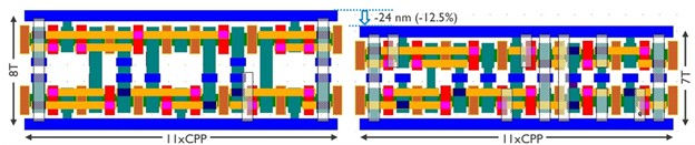
Process Flow and Manufacturing Considerations
The manufacturing process of double-row CEFT involves multiple precise steps that require strict control to achieve optimal results.

This process adopts a monolithic integration approach, forming upper and lower devices through a single active area and gate etching, ensuring precise alignment between stacked devices while reducing manufacturing complexity.
Performance and Scaling Advantages
The double-row CFET architecture exhibits significant improvements in multiples key metrics.

Test results indicate that DR CFET achieves substantial performance improvements while maintaining low power consumption, making it particularly suitable for high-frequency applications with stringent power requirements.
Area Optimization and Implementation
One notable advantage of the double-row CFET architecture is its ability to achieve significant area reduction while maintaining or improving performance.
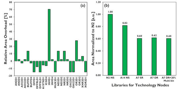
Compared to previous process nodes, DR CFET achieves approximately 40% area scaling potential while offering around 12% power optimization. This optimization is achieved through carefully designed cell heights and efficient utilization of routing resources.
Integration and Scaling
The implementation of DR CFET in SRAM cells represents another significant advancement in semiconductor technology.
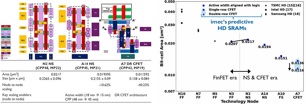
Compared to single-row implementations, DR CFET reduces SRAM area by approximately 15%, which is particularly significant for modern processors where SRAM occupies a large portion of the chip area.
Conclusion
Through design-technology co-optimization, the DR CFET architecture achieves significant advancements in area efficiency, power consumption, and overall performance. Compared to traditional nanosheet devices, this architecture successfully addresses multiple technical challenges. Test results demonstrate approximately 40% area scaling potential while maintaining performance and reducing process complexity.
References
[1] H. Kükner, G. Mirabelli, S. Yang, L. Verschueren, J. Bömmels, J. Y. Lin, D. Abdi, A. Farokhnejad, O. Zografos, N. Horiguchi, M. Garcia Bardon, G. Hellings, and J. Ryckaert, "Double-Row CFET: Design Technology Co-Optimization for Area Efficient A7 Technology Node," in 2024 IEEE International Electron Devices Meeting (IEDM), San Francisco, CA, USA, 2024.
コメント