top of page
Writer's pictureLatitude Design Systems

Designing High-Speed InP DHBT Linear Modulator Drivers for Next-Gen Optical Communications

Introduction

The explosive growth in data traffic fueled by 5G, Internet of Things (IoT), cloud computing, and data centers has necessitated research into higher transmission capacities for optical networks. Multilevel coded transmission formats like Pulse Amplitude Modulation (PAM) and Quadrature Amplitude Modulation (QAM) are of particular interest due to their increased spectral efficiency. However, generating high-symbol-rate multilevel signals electronically while maintaining linearity poses significant challenges. This tutorial discusses the design of a high-performance InP Double Heterojunction Bipolar Transistor (DHBT) linear modulator driver capable of delivering a 3 Vppd PAM-4 output swing at 90 GBaud.

Simplified digital coherent optical fiber transmitter block diagram.
Fig. 1. Simplified digital coherent optical fiber transmitter block diagram.
InP DHBT Technology and Modeling

The modulator driver is implemented in the III-V Lab's 0.5 μm InP DHBT technology featuring cutoff frequencies (fT/fMAX) up to 380/520 GHz (Figure 2) and a breakdown voltage of 4.2V. As shown in Figure 4, InP DHBTs demonstrate superior high-frequency and linearity performance compared to silicon-based technologies, making them attractive for high-symbol-rate large-swing drivers.

0.5-µm InP DHBT fT and fMAX versus collector current, IC, at VCE = 1.6 V, for the three available emitter lengths in the process.
Fig. 2. 0.5-µm InP DHBT fT and fMAX versus collector current, IC, at VCE = 1.6 V, for the three available emitter lengths in the process.
0.5-µm InP DHBT process’ cross-sectional schematic.
Fig. 3. 0.5-µm InP DHBT process’ cross-sectional schematic.
illustrates the state of the art in high-speed technologies by plotting the geometric mean of the cutoff frequency (fT and fMAX) against the breakdown voltage (BVCE0, VDD) for various devices. InP/GaInAs DHBTs are represented by green triangles and InP/Ga(In)AsSb devices by brown diamonds, while SiGe BiCMOS and HBTs are shown as gray circles, and Si CMOS technologies as blue rectangles. Trends for each technology are indicated, with deviations caused by process structural differences like vertical profile variations and 2-D geometry changes, such as narrower emitter widths in HBTs that enhance fMAX by reducing parasitic effects.
Figure 4 illustrates the state of the art in high-speed technologies by plotting the geometric mean of the cutoff frequency (fT and fMAX) against the breakdown voltage (BVCE0, VDD) for various devices. InP/GaInAs DHBTs are represented by green triangles and InP/Ga(In)AsSb devices by brown diamonds, while SiGe BiCMOS and HBTs are shown as gray circles, and Si CMOS technologies as blue rectangles. Trends for each technology are indicated, with deviations caused by process structural differences like vertical profile variations and 2-D geometry changes, such as narrower emitter widths in HBTs that enhance fMAX by reducing parasitic effects.

Accurate DHBT modeling is crucial for reliable IC design, especially at millimeter-wave frequencies where parasitic effects become significant. The conventional deembedding procedure tends to overestimate device parasitics, leading to inaccurate predictions. An improved electromagnetic (EM) simulation-based approach is proposed to extract the small-value external parasitic elements (Figures 5 and 6). This method provides better estimation of canonical cascode gain, stability factor (Figure 8), and the driver's gain response in the 50-110 GHz range, enabling more precise IC design choices.

Top-down view of Ansys HFSS 3-D EM model of the complete triple mesa InP DHBT structure with surrounding groundring. The reference planes for the device model are indicated by dashed lines. For clarity, the outer airbox and substrate layers are not shown.
Fig. 5. Top-down view of Ansys HFSS 3-D EM model of the complete triple mesa InP DHBT structure with surrounding groundring. The reference planes for the device model are indicated by dashed lines. For clarity, the outer airbox and substrate layers are not shown.
Proposed large-signal model structure for InP DHBTs including external parasitics. The dashed box contains the InP DHBT intrinsic part modeled using the modified UCSD HBT model
Fig. 6. Proposed large-signal model structure for InP DHBTs including external parasitics. The dashed box contains the InP DHBT intrinsic part modeled using the modified UCSD HBT model
Simplified schematic of the cascode configuration showing domi nating parasitic elements (bias details not shown). The dashed boxes contain the intrinsic part of the InP DHBTs modeled using the modified UCSD HBT model
Fig. 7. Simplified schematic of the cascode configuration showing domi nating parasitic elements (bias details not shown). The dashed boxes contain the intrinsic part of the InP DHBTs modeled using the modified UCSD HBT model
Simulation comparison of MAG/MSG and the µ stability factor for the cascode configuration with (red broken curves) and without (blue solid curves) external parasitic elements.
Fig. 8. Simulation comparison of MAG/MSG and the µ stability factor for the cascode configuration with (red broken curves) and without (blue solid curves) external parasitic elements.
Comparison of driver's output-stage amplifying cell performances: (a) Schematic of a resistively degenerated cascode differential pair. (b) Schematics of paralleled-transistor amplifying cells. (c) Small-signal differential gain versus frequency, with RE varying in five steps from 0 to 25Ω. (d) Large-signal differential static voltage input-output characteristics of cascode configurations, with RE varied in five steps from 0 to 25Ω.
Fig. 9. Comparison of driver's output-stage amplifying cell performances: (a) Schematic of a resistively degenerated cascode differential pair. (b) Schematics of paralleled-transistor amplifying cells. (c) Small-signal differential gain versus frequency, with RE varying in five steps from 0 to 25Ω. (d) Large-signal differential static voltage input-output characteristics of cascode configurations, with RE varied in five steps from 0 to 25Ω.
Resistively degenerated cascode differential pair half-circuit small-signal equivalent circuit based on a simplified DHBT model.
Fig. 10. Resistively degenerated cascode differential pair half-circuit small-signal equivalent circuit based on a simplified DHBT model.
Linear Driver Design

The linear driver employs a fully differential lumped architecture (Figure 11) with a preamplifier for input matching and a high-gain output stage. The output stage leverages a self-peaking technique (analyzed in Section III.A.2) using a paralleled-transistor cascode with emitter degeneration. This approach boosts the gain-bandwidth product while maintaining large linear output swings (Figure 9).

InP-DHBT linear driver. (a) Block diagram. (b) Schematic.
Fig. 11. InP-DHBT linear driver. (a) Block diagram. (b) Schematic.

The self-peaking mechanism stems from the synergistic effects of emitter degeneration and transistor capacitances (Equation 2), providing high-frequency gain enhancement. Optimal transistor dimensions and degeneration resistances are chosen to position the peaking frequencies (f2 and f4) within the desired bandwidth while mitigating impedance matching degradation from excessive transistor capacitances.

The preamplifier features a linear cascode amplifier with custom emitter degeneration for common-mode rejection. The output stage utilizes a two-paralleled-transistor differential cascode with 7 μm common-base and 10 μm "common-emitter" DHBTs for optimal gain-bandwidth product and linearity. Inductive peaking networks (Figure 12) further extend the bandwidth and improve output matching.

InP-DHBT linear driver output inductive peaking optimization. LC’s length is varied from 0 to 80 µm with a 10-µm step. (a) S-parameter gain, S21. (b) S-parameter output reflection coefficient, S22.
Fig. 12. InP-DHBT linear driver output inductive peaking optimization. LC’s length is varied from 0 to 80 µm with a 10-µm step. (a) S-parameter gain, S21. (b) S-parameter output reflection coefficient, S22.
Experimental Results

The linear driver chip (Figure 13) exhibits a measured bandwidth exceeding 110 GHz with 13 dB of peaking gain at 95 GHz (Figure 15a). Input and output return losses remain below -10 dB up to 92 and 95 GHz, respectively, demonstrating wideband impedance matching. The reverse isolation (S12) is below -35 dB, ensuring stability.

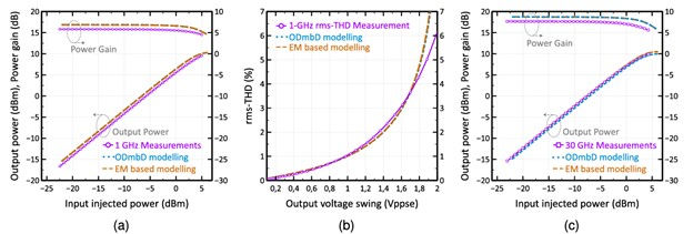
Large-signal continuous wave measurements at 1 GHz show a 9.1 dBm (3.6 Vppd) output power at 1 dB gain compression with 5.8 dB gain (Figure 16a). At 30 GHz, the gain increases to 7.2 dB due to peaking. The RMS total harmonic distortion is 2.7% at 3 Vppd output swing (Figure 16b), highlighting the driver's excellent linearity.

0.5-µm InP-DHBT linear driver chip microphotograph.
Fig. 13. 0.5-µm InP-DHBT linear driver chip microphotograph.
the impact of different InP-DHBT modeling techniques on the performance of a linear driver. The brown curve network represents EM-based DHBT modeling, and the green curve network represents ODmbD DHBT modeling. The inductor coil's (LC) length varies from 0 to 80 µm in 10-µm increments. Subfigure (a) shows the S-parameter gain, S21, while subfigure (b) details the S-parameter output reflection coefficient, S22.
Figure 14 compares the impact of different InP-DHBT modeling techniques on the performance of a linear driver. The brown curve network represents EM-based DHBT modeling, and the green curve network represents ODmbD DHBT modeling. The inductor coil's (LC) length varies from 0 to 80 µm in 10-µm increments. Subfigure (a) shows the S-parameter gain, S21, while subfigure (b) details the S-parameter output reflection coefficient, S22.

Digital PAM-4 measurements at 75 and 90 GBaud reveal clear eye openings (Figure 18), even without digital signal processing (DSP) or post-processing. EM-circuit co-simulations accurately predict the measured small-signal, large-signal CW, and digital PAM-4 performance, validating the improved modeling approach (Figures 15, 16, and 19).

single-ended S-parameter measurements for an InP-DHBT linear driver, shown with magenta symbols. The figure includes results from EM-circuit cosimulations using two types of InP-DHBT modeling: EM-based (orange dashed lines) and ODmbD (blue dotted lines). It covers various parameters: (a) Gain (S21) and input reflection (S11), (b) Output reflection (S22), (c) Reverse gain (S12), (d) µ stability factor, (e) Group delay, and (f) Common mode rejection ratio, all derived from S-parameter measurements.
Figure 15 presents single-ended S-parameter measurements for an InP-DHBT linear driver, shown with magenta symbols. The figure includes results from EM-circuit cosimulations using two types of InP-DHBT modeling: EM-based (orange dashed lines) and ODmbD (blue dotted lines). It covers various parameters: (a) Gain (S21) and input reflection (S11), (b) Output reflection (S22), (c) Reverse gain (S12), (d) µ stability factor, (e) Group delay, and (f) Common mode rejection ratio, all derived from S-parameter measurements.
single-ended large-signal continuous wave measurements for an InP-DHBT linear driver, represented by magenta solid lines with symbols. It includes results from EM-circuit cosimulation using two modeling approaches: EM-based (orange dashed lines) and ODmbD (blue dotted lines). The measurements cover: (a) Output power and power gain relative to input power at 1 GHz, (b) RMS-total harmonic distortion against output voltage swing at 1 GHz, and (c) Output power and power gain relative to input power at 30 GHz.
Figure 16 shows single-ended large-signal continuous wave measurements for an InP-DHBT linear driver, represented by magenta solid lines with symbols. It includes results from EM-circuit cosimulation using two modeling approaches: EM-based (orange dashed lines) and ODmbD (blue dotted lines). The measurements cover: (a) Output power and power gain relative to input power at 1 GHz, (b) RMS-total harmonic distortion against output voltage swing at 1 GHz, and (c) Output power and power gain relative to input power at 30 GHz.
InP-DHBT linear driver high-symbol-rate PAM-4 characterization environment.
Fig. 17. InP-DHBT linear driver high-symbol-rate PAM-4 characterization environment.
differential PAM-4 output eye diagrams from an InP-DHBT linear driver. Subfigure (a) shows a 3-Vppd, 75-GBd (150-Gb/s) output signal, with an inset featuring the active combiner's 830-mVppd, 75-GBd output signal measured before connection to the driver. Subfigure (b) illustrates a 3-Vppd, 90-GBd (180-Gb/s) output signal, with a corresponding inset of the active combiner's 830-mVppd, 90-GBd output signal measured pre-connection.
Figure 18 displays differential PAM-4 output eye diagrams from an InP-DHBT linear driver. Subfigure (a) shows a 3-Vppd, 75-GBd (150-Gb/s) output signal, with an inset featuring the active combiner's 830-mVppd, 75-GBd output signal measured before connection to the driver. Subfigure (b) illustrates a 3-Vppd, 90-GBd (180-Gb/s) output signal, with a corresponding inset of the active combiner's 830-mVppd, 90-GBd output signal measured pre-connection.
InP-DHBT linear driver large-signal digital measurements and tran sient EM-circuit cosimulation comparison at 75 GBd in PAM-4. Simulations use (a) ODmbD InP-DHBT modeling and (b) EM-based InP-DHBT modeling.
Fig. 19. InP-DHBT linear driver large-signal digital measurements and tran sient EM-circuit cosimulation comparison at 75 GBd in PAM-4. Simulations use (a) ODmbD InP-DHBT modeling and (b) EM-based InP-DHBT modeling.
Conclusion

This tutorial presented the design and characterization of a high-performance InP DHBT linear modulator driver for next-generation optical communications. The driver leverages an improved EM-based DHBT modeling approach and a self-peaking output stage to deliver a 3 Vppd PAM-4 output swing at 90 GBaud with a bandwidth exceeding 110 GHz. The design methodology, theoretical analysis, and experimental results highlight the potential of InP DHBTs in enabling Tb/s-class optical transceivers and emerging applications like 6G wireless.

Reference

[1] R. Hersent et al., "InP DHBT Linear Modulator Driver With a 3-Vppd PAM-4 Output Swing at 90 GBaud: From Enhanced Transistor Modeling to Integrated Circuit Design," in IEEE Transactions on Microwave Theory and Techniques, vol. 72, no. 3, pp. 1618-1631, March 2024.

Comments


bottom of page