
CMOS-Integrated Piezoelectric MEMS PDK Solution
- Latitude Design Systems
- Mar 27
- 3 min read
Introduction
The integration of piezoelectric MEMS with CMOS technology represents a significant advancement in microsystems engineering. Compared to traditional CMOS processes with well-established Process Design Kits (PDKs), the integration of piezoelectric MEMS lacks a standardized design framework. This paper explores a comprehensive PDK solution for the integration of piezoelectric MEMS with CMOS technology, focusing on processes based on aluminum nitride (AlN) [1].

Process Architecture and Layer Stacking
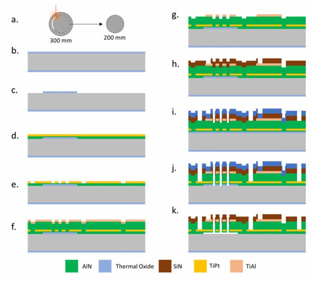
The fundamental architecture consists of carefully selected layers that support multiple device functionalities. This process was developed at the Cornell NanoScale Science and Technology Facility (CNF) and comprises six fundamental layers. From bottom to top, the layer composition includes a silicon dioxide release layer (1000 nm), an aluminum nitride buffer layer for electrical insulation (50 nm), a bottom titanium/platinum electrode (100/20 nm), an aluminum nitride piezoelectric layer (0.5, 1, and 1.5 μm), a top titanium/aluminum electrode (200/20 nm), and a top silicon nitride buffer layer (300-900 nm).

Device Integration and Layout Design
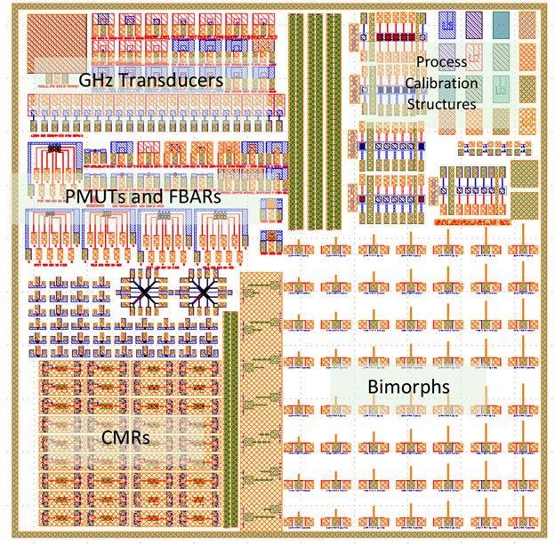
The process enables the integration of multiple device types on a single platform, demonstrating the versatility of the solution. The layout uses a 10 x 10 mm mask size to accommodate various device configurations. The entire design includes GHz transducers, PMUTs, CMRs, FBARs, and process calibration structures, achieving high integration through optimized layout design.
Manufacturing Process
The manufacturing process employs a series of advanced techniques to ensure precise device formation. The ASML 248 nm deep ultraviolet (DUV) lithography process, combined with UV210 deep ultraviolet positive photoresist and UV42P anti-reflective coating, achieves high-resolution patterning. Multi-step ion beam etching is used for electrode patterning, with stress-adjusted aluminum nitride deposition through a Stress Adjustment Unit (SAU) and silicon nitride layer deposition via PECVD. The precise control of these process steps ensures the final device's performance and reliability.
Device Implementation and Results
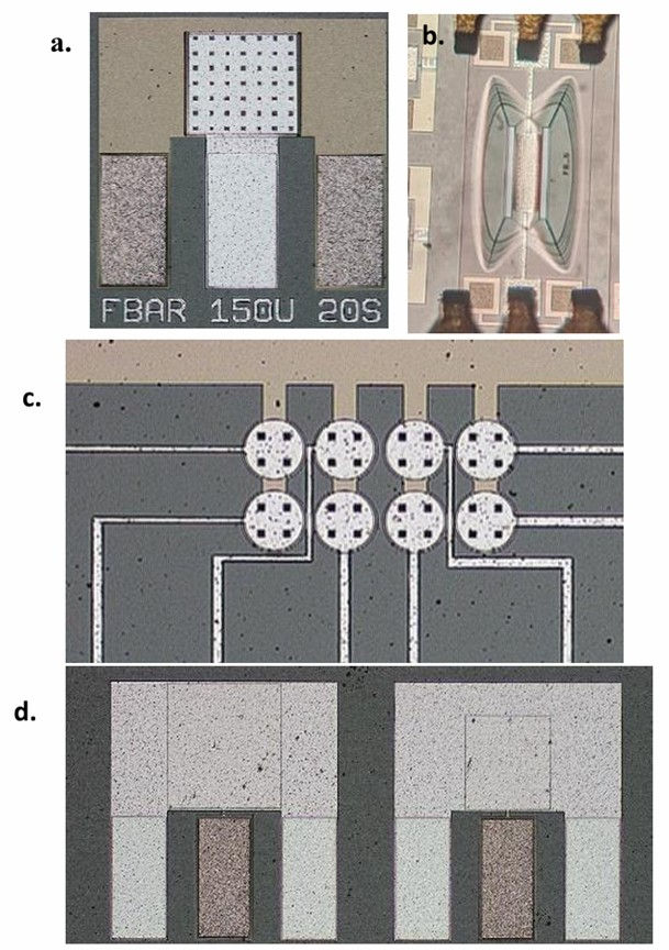
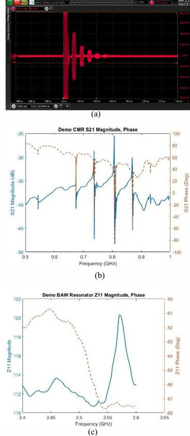
The process successfully demonstrated the realization of multiple device types. The GHz transducer achieved an echo amplitude exceeding 80mVpp, the FBAR resonator reached the designed frequency of 2.5 GHz, and the CMR device exhibited the expected 800 MHz resonance characteristics. While the PMUTs demonstrate structural integrity, further optimization is required to improve yield. These results validate the feasibility and performance potential of the process solution.
Future Development
Several key improvement areas exist for the further advancement of this technology. Process improvements should include implementing patterned release layers, integrating via connections between electrodes, developing frequency tuning capabilities, and optimizing stress control in suspended structures. PDK development requires creating a comprehensive layout environment, implementing Design Rule Checking (DRC) and Layout vs. Schematic (LVS) verification, developing accurate simulation models, and generating an automated parameterized cell library.
The successful realization of this process demonstrates the feasibility of creating a unified platform for the integration of piezoelectric MEMS and CMOS technology. This advancement is expected to make complex MEMS designs more accessible, like how standard CMOS PDKs transformed integrated circuit design. This paper outlines the fundamental framework for piezoelectric MEMS integration, with the successful realization of multiple device types confirming the versatility and commercial potential of this approach.
Reference
[1] B. Davaji, J. Kuo, M. Rinaldi, and A. Lal, "Towards a CMOS Integrated Piezoelectric MEMS Process Design Kit," in Solid-State Sensors, Actuators, and Microsystems Workshop, Hilton Head Island, SC, USA, Jun. 5-9, 2022, pp. 31-34, doi: 10.31438/trf.hh2022.7.
Comments