
A Low-Power High-Bandwidth PAM4 VCSEL Driver with Three-Tap FFE
- Latitude Design Systems

- Apr 30, 2024
- 4 min read
Introduction
The ever-increasing demand for higher data rates in internet traffic, cloud computing, and emerging technologies like 5G and AI has fueled the need for high-speed optical interconnects. Short-reach optical interconnects based on Vertical Cavity Surface Emitting Lasers (VCSELs) are an attractive solution for 400Gb/s Ethernet systems commonly used in data centers. However, designing VCSEL drivers poses several challenges related to the VCSEL's bandwidth limitations, bias-dependent frequency response, static and dynamic nonlinearities.
This tutorial presents a low-power high-bandwidth PAM4 VCSEL transmitter that addresses these challenges through circuit and architecture innovations. We introduce a new cascode voltage-mode driver structure that provides larger output modulation current with smaller devices and lower power compared to conventional drivers. An asymmetric three-tap feedforward equalizer (FFE) is employed to compensate for the VCSEL's bandwidth and nonlinearity. The driver is also implemented using multiple segments to optimize output impedance and linearity.
VCSEL Characteristics and Challenges
The frequency response of a VCSEL is dependent on its bias current. The VCSEL bandwidth is proportional to (Idc - Ith)1/2, where Idc and Ith are the bias and threshold currents, respectively. At low bias, the damping factor is low, resulting in relaxation oscillations in the step response. Increasing bias reduces overshoot but increases power consumption.
VCSELs also exhibit static nonlinearity, where the relationship between output power and bias current becomes nonlinear at high currents due to saturation effects. Dynamic nonlinearity relates to the dependence of bandwidth and frequency response on the instantaneous VCSEL current.
When using PAM4 signaling, the static nonlinearity deteriorates the level separation between the four levels. Dynamic nonlinearity causes timing misalignment and asymmetry in the optical eye diagram, effects that worsen at lower VCSEL bias.
Proposed PAM4 VCSEL Driver Architecture
The proposed PAM4 VCSEL transmitter, shown in Figure 1, introduces several innovations to address the above challenges while achieving low power consumption.

New Cascode Voltage-Mode Driver
A new cascode voltage-mode (VM) driver structure is proposed, as shown in Figure 2(e). Compared to the conventional VM driver in Figure 2(a), this new structure uses two high-pass RC filters to apply voltage pulses to the gates of the cascode devices during transitions. These pulses enhance the rise and fall times. Additionally, auxiliary transistors M9 and M10 improve the output voltage swing by providing auxiliary pull-up and pull-down paths.

This new driver achieves a larger modulation current (2.5x compared to a conventional cascode driver) while using smaller devices and lower power, as verified by simulations in Figures 3 and 4. The ability to use smaller devices reduces the self-loading capacitance, relaxing bandwidth limitations.


Asymmetric Three-Tap FFE
To compensate for the VCSEL's bandwidth and nonlinearity, the proposed transmitter employs an asymmetric three-tap FFE, as shown in Figure 5(a). The equalizer has independent tap weights for the most significant bit (MSB) and least significant bit (LSB) paths, as well as different weights for rise and fall transitions. This asymmetry effectively compensates for the VCSEL's dynamic nonlinearity.

The main cursor tap equalizes the VCSEL's static nonlinearity, while the pre-cursor and post-cursor taps equalize the dynamic nonlinearity. Tunable analog delay cells realize the FFE taps, with tap voltages provided off-chip.
Multi-Segment Driver Implementation
The driver is implemented using three segments, each with a separate switch to optimize the output impedance and linearity, as depicted in Figure 6. Enabling all segments maximizes bandwidth by varying the driver's output resistance to an optimum range. Each segment includes the asymmetric FFE taps, ensuring consistent equalization regardless of the number of enabled segments.

Backend and Optical Integration
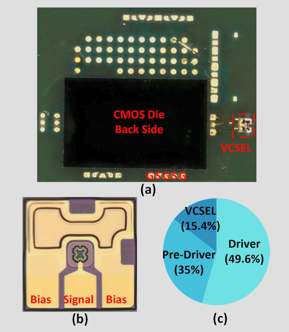
The driver is DC-coupled to the VCSEL to avoid large bypass capacitors that would degrade bandwidth (Figure 10). A current mirror structure provides the VCSEL's DC bias. The transmitter is implemented in a 12nm CMOS FinFET process and packaged for optical measurements using a commercial 850nm VCSEL, as shown in Figures 7 and 8.


Measurement Results
Electrical Measurements
Based on electrical measurements using a 50Gb/s PRBS-9 NRZ input, the transmitter achieves a 160mV swing voltage with a 50mV eye-opening for NRZ signaling (Figure 9(a)). With independent 32Gb/s PRBS-9 NRZ inputs for MSB and LSB, a PAM4 eye diagram with >18mV opening is obtained at 64Gb/s (Figure 9(b)).

Optical Measurements
Optical measurements are performed by wirebonding the CMOS die to a commercial 850nm VCSEL (Figure 10). At 50Gb/s PAM4 operation, the proposed transmitter achieves an optical modulation amplitude (OMA) of 1.43dBm and an extinction ratio of 3.9dB, exceeding the 100GBASE-SR requirements of -7dBm OMA and 2dB ER (Figure 11(b)). The measured PAM4 RLM is 0.95.


The total power consumption is 48.5mW from 1V, 2V, and -1.5V supplies at 50Gb/s PAM4 operation, including all transmitter circuits. This corresponds to a power efficiency of 0.97pJ/b, making it one of the most power-efficient PAM4 VCSEL drivers reported, as shown in the comparison in Figure 1.
Conclusion
This tutorial presented a low-power high-bandwidth PAM4 VCSEL driver that introduces a new cascode voltage-mode driver structure, an asymmetric three-tap FFE, and a multi-segment implementation. These innovations enable large modulation currents, VCSEL bandwidth extension, and static/dynamic nonlinearity compensation while using small devices and low power. Implemented in 12nm CMOS FinFET, the transmitter achieves 50Gb/s PAM4 and 40Gb/s NRZ operation with high OMA, ER, and excellent power efficiency of 0.97pJ/b, making it suitable for high-speed optical interconnects in data centers.
Reference
[2] M. Haghi Kashani, H. Shakiba, and A. Sheikholeslami, "A Low-Power High-BW PAM4 VCSEL Driver With Three-Tap FFE in 12-nm CMOS FinFET Process," IEEE Journal of Solid-State Circuits, accepted Apr. 1, 2024.


Comments