
3D Photonics Integration Technology for Ultra-Low Energy, High Bandwidth-Density Chip Data Links
- Latitude Design Systems
- Feb 20
- 3 min read
Introduction
The rapid advancement of artificial intelligence (AI) has placed extremely high demands on high-speed, low-power data communication between computing nodes. While AI chip computational capabilities have significantly improved, the development of the network interconnecting these chips has lagged, creating a critical bottleneck. This paper introduces a breakthrough solution leveraging 3D-integrated photonics technology to achieve ultra-low energy, high bandwidth chip-to-chip communication [1].
Overview of Technical Challenges
Over the past two decades, chip computing speeds have increased 1,000 times faster than communication bandwidth. Currently, the energy cost of data transmission is approximately 100 times higher than that of computational operations, severely limiting the improvement of AI performance. Electrical interconnects between traditional chips rely on centimeter-scale wires, which are slow and energy-intensive. Overcoming this limitation requires the conversion from electrical to optical signals within a compact area inside the chip.
Advantages of 3D Integration

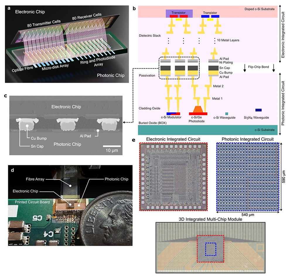
The solution lies in the 3D-integrated photonic chips, where a 28nm CMOS electronic chip is combined with a photonics chip containing optical devices. The electronic chip, fabricated using 28nm CMOS technology, ensures optimal energy efficiency. Meanwhile, the photonic chip integrates silicon-based optical devices, such as microring resonator modulators and photodetectors.
The two chips are bonded using Cu-Sn micro-bumps, achieving an extremely small 15μm pitch and 10μm bump diameter in an array of 2304 interconnections. This high-density integration enables high unprecedented bandwidth density while maintaining low capacitance.
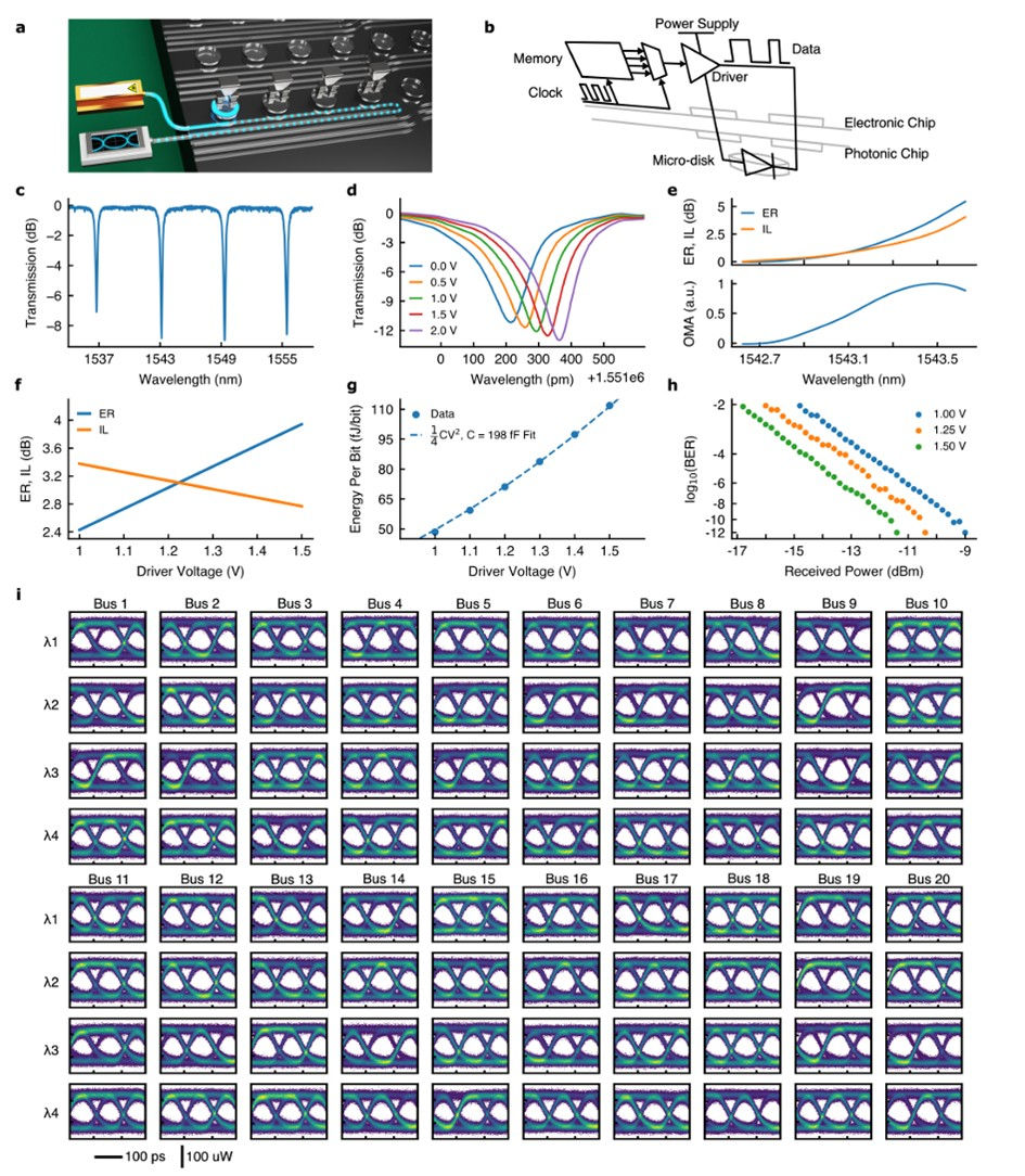
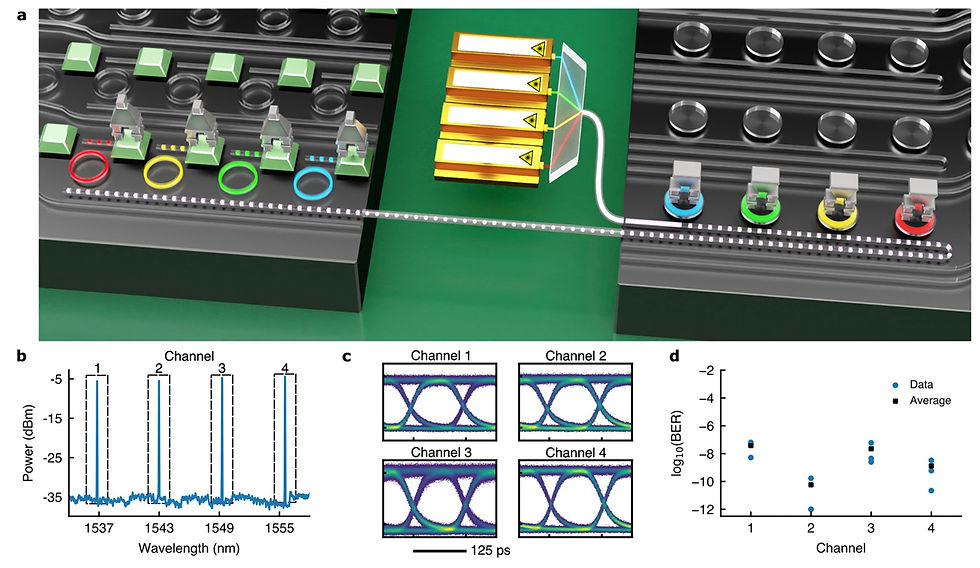
The system consists of 80 parallel transmitter units and 80 receiver units, organized into 20 waveguide buses, each supporting 4 wavelength channels. The transmitter units encode electrical data onto an optical signal carrier using microring resonator modulators. These modulators achieve an ultra-low energy consumption of 50 fJ/bit at a 1V drive swing.

The receiver units employ microring resonators to filter specific wavelengths onto germanium photodiodes, efficiently converting optical signals back into electrical currents. The receiver circuitry consumes only 70 fJ/bit to amplify these signals at a data rate of 10 Gbps.
System Performance and Impact
The system achieves groundbreaking performance metrics:
Total energy consumption: 120 fJ/bit
Bandwidth density: 5.3 Tbps/mm²
Total bandwidth: 800 Gbps
Compact footprint: Only 0.32 mm²
10^-12 Error-free operation with BER < 10⁻¹²
Compared to previous technologies, both energy efficiency and bandwidth density have doubled. Furthermore, both chips are fabricated using commercial CMOS foundries, ensuring large-scale manufacturability.
Applications and Future Impact
This technology eliminates data location constraints, enabling AI computing at unprecedented scales. The ultra-efficient optical link allows processors to communicate over long distances with minimal energy consumption. This capability revolutionizes computing architecture by:
Interconnecting distributed computing resources via optical networks
Significantly scaling up distributed AI systems
Flexibly allocating memory and processing resources
Optimizing data center architectures for AI workloads
As AI continues to drive computational demands, this breakthrough in chip-to-chip communication lays the foundation for scalable AI system expansion. The combination of ultra-low energy, high bandwidth density, and manufacturability makes this an effective solution for addressing fundamental challenges in AI system development.
Beyond AI, this technology has broad applications in high-performance computing, telecommunications, and any domain requiring high-bandwidth, energy-efficient chip interconnects. By bridging the gap between computing and communication capabilities, this work paves the way for the future of advanced computing systems.
References
[1] S. Daudlin et al., "3D photonics for ultra-low energy, high bandwidth-density chip data links," arXiv:2310.01615v1 [physics.optics], Oct. 2023.
コメント